
User manual


Hardware Description
2010 Microchip Technology Inc. DS51845B-page 13
1.4 ANALOG INPUT STRUCTURE
Two differential input paths allow external signal sources to be easily connected to the
MCP3901 input. Edge connectors JP1 and JP2 are 3-pin connectors that act both as
crew type and clip on post connectors.
JP1 and JP2 can be used to force either channel from a differential to single-ended
configuration. R3 and R4 (on CH0), and R1 and R2 (on CH2) act as locations for
burden resistor connectors for any current transformer inputs.
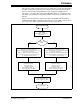
1.5 UNIVERSAL SERIAL BUS (USB)
The MCP3901 ADC Evaluation Board for 16-Bit MCUs also contains a USB connection
for higher speed sampling and data collection. The circuit includes a 512x8 SRAM for
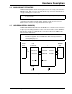
data collection. Figure 1-5 summarizes the connections between the ADC, the two
microcontrollers and memory.
FIGURE 1-5: USB Block Diagram.
Note: To use an edge connector as a post connector, pull up the blue plastic top
to access posts.
Note: For the MCP3901 ADC Evaluation Board for 16-Bit MCUs release, no USB
firmware is supplied. The PIC18F86J55 is blank and only included for
development purposes.
SCK2/RG6
SDI2/RG7
SDO2/RG8
SS
2/RG9
USB
RD6/SCK2
RD4/SDO2
RD5/SDI2
PIC18F86J55
RD7/SS
2
ADC
MCP3901
RF6/SCK1
RF7/SDI1
RF8/SDO1
SCK
SDO
SDI
USB
SERIAL
512x8
SRAM
8
I