
Datasheet


MCP3901 LOW-COST POWER
MONITOR REFERENCE DESIGN
2010 Microchip Technology Inc. DS51915A-page 11
Chapter 2. Installation and Operation
2.1 POWER MONITOR FIRMWARE DESCRIPTION
2.1.1 Samples Acquisition
Using the external ADC, the current and voltage samples must be acquired before the
correct values of the desired parameters can be computed. The MCU reads the values
of the samples from the ADC through the SPI bus.
The sampling speed of the ADC is controlled by the clock frequency of the MCP3901.
The MCU uses the Output Compare 1 module to generate a 50% pulse-width
modulation (PWM) signal that has a frequency of 901.120 kHz. This frequency can be
easily changed by modifying values in the Timer2 Period Register (PR2) and the
Compare Register 1 (CCPR1).
The sampling speed of the ADC is 1024 times lower than the master clock in the
MCP3901, meaning 880 sps at an Over Sampling Rate (OSR) of 256.
2.1.2 Signal Processing
In order to obtain the desired parameter values out of the acquired samples, a signal
processing technique must be assumed. Since this design uses an 8-bit MCU, the
signal processing technique that is implemented must be fast enough to avoid limiting
the sampling speed, so that a time-domain analysis can be performed. The signal
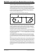
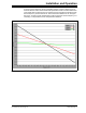
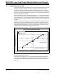
processing technique is graphically described in Figure 2-1.
FIGURE 2-1: Block Diagram of the Signal Processing Algorithm.
Initially, the acquired samples go through a first-order Infinite Impulse Response
high-pass filter (IIR HPF), which has the following roles:
1. Removes the offset of the ADC
2. Compensates for the Sinc filters transfer function
LPF
LPF
Voltage Sample
Current Sample
HPF
HPF
Active Power
Apparent Power
U
RMS
I
RMS
Active Power Scaling Factor
RMS Current Scaling Factor
RMS Voltage Scaling Factor
LPF
SQRT
SQRT
Power Factor
LPF
LPF
LPF