
User manual
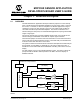

Hardware Description
© 2006 Microchip Technology Inc. DS51609A-page 11
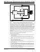
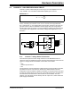
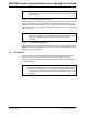
2.4 CHANNEL 2 - HIGH-PRECISION GAIN CIRCUIT
Channel 2 contains a differential gain circuit using a low noise amplifier from Cirrus
Logic, CS3002. The noise allows a differential amplifier gain of 103 V/V.
EQUATION 2-1:
This was chosen so that the amplifier noise would be similar to that of the MCP3551
device, maximizing the resolution of the circuit. The board comes populated with
R
G
=100Ω and R
F
= 5.1 kΩ. Higher gains can be chosen, however in this case, the
gain was chosen to allow for headroom near the supply rails (+5V and ground) to
handle a large variety of sensors. For more information regarding gain selection and
circuit results, refer to application note AN1030, “Weigh Scale Applications for the
MCP3551”.
FIGURE 2-5: High Gain Circuit Using CS3002.
2.4.1 Channel 2 - Voltage Reference Selection
There are three options to select voltage reference for the MCP355X device for
channel 2. This is accomplished using the 14-pin dual row header JP2. There are three
options for voltage reference evaluation on the bottom of this header.
•V
REF
• PICmicro port pin RC6-7
•V
DD
The first selection uses the stand-alone voltage reference circuit included on the board,
populated with the low noise reference LM4140 from National Semiconductor
®
Corporation.The second selection allows for evaluation of using the PICmicro port pins
to supply the voltage reference for the circuit. The board uses two pins of the PICmicro
microcontroller for increased drive, RC6 and RC7 of the PIC16F877. The third
selection, V
DD
, will supply the V
REF
directly from the output of JP1, which selects the
power supply for the board.
G12
R
F
R
G
-------
〈〉+=
-SENSE
-IN
-OUT
+OUT
+IN
+SENSE
P7
+
-
+
-
MCP3551
R
G
R
F
CS3002
U6
GAIN-
DIRECT-
DIRECT+
GAIN+
VREF
RC7
JP2
VDD
V
IN-
V
IN+
V
REF