
User manual

Quick Start Instructions
© 2009 Microchip Technology Inc. DS51787A-page 7
1.3 GETTING STARTED WITH PICKIT™ SERIAL ANALYZER
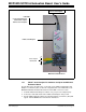
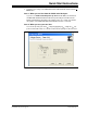
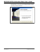
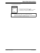
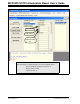
Figure 1-1 shows the MCP3425 SOT23-6 Evaluation Board, while Figure 1-2 shows
the evaluation board and the PICkit Serial Analyzer connection.
The following instructions show how to use them together:
1. Connect the MCP3425 SOT23-6 Evaluation Board’s J1 pin socket to the PICkit
Serial Analyzer, as shown in Figure 1-2.
2. Connect oscilloscope probes to SCL and SDA test pins (optional).
3. V
DD
selection: You can use the V
DD
from the PICkit Serial Analyzer or your own
external V
DD
. You can select the V
DD
path using the JP1 connector:
(a) Connect JP1, if using V
DD
from PICkit Serial Analyzer.
(b) Disconnect JP1 and apply V
DD
at the V
DD
pad, if you are using external V
DD
.
4. Connect V
DD
, if external V
DD
is used.
5. LED D1 is turned on when V
DD
is applied.
6. Connecting analog inputs: If you need to measure single-ended input, connect
the unused pin (for example, V
IN
-) to V
SS
.
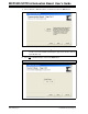
7. Use the PICkit Serial Analyzer PC GUI to send I
2
C write and read commands.
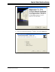
See Section 1.3.2.1 “Creating a Script File for Configuration Byte Writing”
8. Execute the PICkit Serial Analyzer Script file and obtain the ADC conversion
results. The conversion results appear on the PICkit Serial Analyzer PC GUI. You
can also observe the conversion results using the oscilloscope.
Note: If you are using external V
DD
, connect the external V
DD
at V
DD
pad.
Note: Do not connect V
DD
if you are using the V
DD
from the PICkit Serial
Analyzer. The PICkit Serial Analyzer provides the V
DD
automatically if it is
connected to the PC.
Note: If the V
DD
is provided from the PICkit Serial Analyzer, then the LED may not
be turned on until you execute a command. See Section 1.3.2.1 “Creating
a Script File for Configuration Byte Writing” for executing the I
2
C
command.
CAUTION
The analog input pin has ESD diodes. Certain input conditions can damage the
device. Please pay attention to the following conditions:
(a) Do not apply input greater than the input range specified by the MCP3425
data sheet.
(b) Apply input signal after the V
DD
is powered-up.