
Datasheet
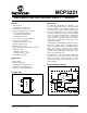


MCP3221
DS21732D-page 4 2002-2013 Microchip Technology Inc.
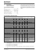
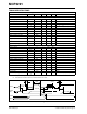
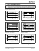
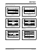
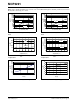
TIMING SPECIFICATIONS
FIGURE 1-1: Standard and Fast Mode Bus Timing Data.
Electrical Characteristics: All parameters apply at V
DD
= 2.7V - 5.5V, V
SS
= GND, T
AMB
= -40°C to +85°C.
Parameters Sym Min Typ Max Units Conditions
I
2
C Standard Mode
Clock frequency f
SCL
0 — 100 kHz
Clock high time T
HIGH
4000 — — ns
Clock low time T
LOW
4700 — — ns
SDA and SCL rise time T
R
— — 1000 ns From V
IL
to V
IH
(Note 1)
SDA and SCL fall time T
F
— — 300 ns From V
IL
to V
IH
(Note 1)
START condition hold time T
HD:STA
4000 — — ns
START condition setup time T
SU:STA
4700 — — ns
Data input setup time T
SU:DAT
250 — — ns
STOP condition setup time T
SU:STO
4000 — — ns
STOP condition hold time T
HD:STD
4000 — — ns
Output valid from clock T
AA
— — 3500 ns
Bus free time T
BUF
4700 — — ns Note 2
Input filter spike suppression T
SP
— — 50 ns SDA and SCL pins (Note 1)
I
2
C Fast Mode
Clock frequency F
SCL
0 — 400 kHz
Clock high time T
HIGH
600 — — ns
Clock low time T
LOW
1300 — — ns
SDA and SCL rise time T
R
20 + 0.1C
B
— 300 ns From V
IL
to V
IH
(Note 1)
SDA and SCL fall time T
F
20 + 0.1C
B
— 300 ns From V
IL
to V
IH
(Note 1)
START condition hold time T
HD:STA
600 — — ns
START condition setup time T
SU:STA
600 — — ns
Data input hold time T
HD:DAT
0—0.9ms
Data input setup time T
SU:DAT
100 — — ns
STOP condition setup time T
SU:STO
600 — — ns
STOP condition hold time T
HD:STD
600 — — ns
Output valid from clock T
AA
— — 900 ns
Bus free time T
BUF
1300 — — ns Note 2
Input filter spike suppression T
SP
— — 50 ns SDA and SCL pins (Note 1)
Note 1: This parameter is periodically sampled and not 100% tested.
2: Time the bus must be free before a new transmission can start.
T
F
T
HIGH
V
HYS
T
R
T
SU:STA
T
SP
T
HD:STA
T
LOW
T
HD:DAT
T
SU:DAT
T
SU:STO
T
BUF
T
AA
SCL
SDA
IN
SDA
OUT