
Datasheet


2002-2013 Microchip Technology Inc. DS21732D-page 3
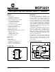
MCP3221
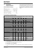
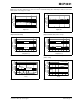
TEMPERATURE SPECIFICATIONS
Power Requirements
Operating Voltage V
DD
2.7 — 5.5 V
Conversion Current I
DD
— 175 250 µA
Standby Current I
DDS
— 0.005 1 µA SDA, SCL = V
DD
Active bus current I
DDA
——120µANote 4
Conversion Rate
Conversion Time t
CONV
—8.96—µsNote 5
Analog Input Acquisition Time t
ACQ
—1.12—µsNote 5
Sample Rate f
SAMP
— — 22.3 ksps f
SCL
= 400 kHz (Note 1)
Electrical Characteristics: Unless otherwise noted, all parameters apply at V
DD
= 5.0V, V
SS
= GND.
Parameters Symbol Min Typ Max Units Conditions
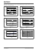
Temperature Ranges
Industrial Temperature Range T
A
-40 — +85 °C
Extended Temperature Range T
A
-40 — +125 °C
Operating Temperature Range T
A
-40 — +125 °C
Storage Temperature Range T
A
-65 — +150 °C
Thermal Package Resistances
Thermal Resistance, 5L-SOT23
JA
—
256
—
°C/W
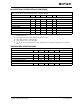
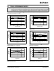
DC ELECTRICAL SPECIFICATIONS (CONTINUED)
Electrical Characteristics: Unless otherwise noted, all parameters apply at V
DD
= 5.0V, V
SS
= GND, R
PU
= 2 k
T
AMB
= -40°C to +85°C, I
2
C Fast Mode Timing: f
SCL
= 400 kHz (Note 3).
Parameters Sym Min Typ Max Units Conditions
Note 1: “Sample time” is the time between conversions once the address byte has been sent to the converter.
Refer to Figure 5-6.
2: This parameter is periodically sampled and not 100% tested.
3: R
PU
= Pull-up resistor on SDA and SCL.
4: SDA and SCL = V
SS
to V
DD
at 400 kHz.
5: t
ACQ
and t
CONV
are dependent on internal oscillator timing. See Figure 5-5 and Figure 5-6 for relation to
SCL.