
Datasheet
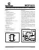


MCP3221
DS21732D-page 2 2002-2013 Microchip Technology Inc.
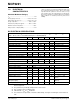
1.0 ELECTRICAL
CHARACTERISTICS
Absolute Maximum Ratings †
V
DD
...................................................................................7.0V
Analog input pin w.r.t. V
SS
.......... ............. -0.6V to V
DD
+0.6V
SDA and SCL pins w.r.t. V
SS
........... .........-0.6V to V
DD
+1.0V
Storage temperature .....................................-65°C to +150°C
Ambient temp. with power applied ................-65°C to +125°C
Maximum Junction Temperature...................................150°C
ESD protection on all pins (HBM) ................................. 4kV
† Stresses above those listed under “Maximum ratings” may
cause permanent damage to the device. This is a stress rating
only and functional operation of the device at those or any
other conditions above those indicated in the operational list-
ings of this specification is not implied. Exposure to maximum
rating conditions for extended periods may affect device
reliability.
DC ELECTRICAL SPECIFICATIONS
Electrical Characteristics: Unless otherwise noted, all parameters apply at V
DD
= 5.0V, V
SS
= GND, R
PU
= 2 k
T
AMB
= -40°C to +85°C, I
2
C Fast Mode Timing: f
SCL
= 400 kHz (Note 3).
Parameters Sym Min Typ Max Units Conditions
DC Accuracy
Resolution 12 bits
Integral Nonlinearity INL — ±0.75 ±2 LSB
Differential Nonlinearity DNL — ±0.5 ±1 LSB No missing codes
Offset Error — ±0.75 ±2 LSB
Gain Error — -1 ±3 LSB
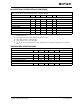
Dynamic Performance
Total Harmonic Distortion THD — -82 — dB V
IN
= 0.1V to 4.9V @ 1 kHz
Signal-to-Noise and Distortion SINAD — 72 — dB V
IN
= 0.1V to 4.9V @ 1 kHz
Spurious-Free Dynamic Range SFDR — 86 — dB V
IN
= 0.1V to 4.9V @ 1 kHz
Analog Input
Input Voltage Range V
SS
-0.3 — V
DD
+0.3 V 2.7V V
DD
5.5V
Leakage Current -1 — +1 µA
SDA/SCL (open-drain output):
Data Coding Format Straight Binary
High-level input voltage V
IH
0.7 V
DD
——V
Low-level input voltage V
IL
— — 0.3 V
DD
V
Low-level output voltage V
OL
——0.4VI
OL
= 3 mA, R
PU
= 1.53 k
Hysteresis of Schmitt trigger inputs V
HYST
—0.05V
DD
—Vf
SCL
= 400 kHz only
Input leakage current I
LI
-1 — +1 µA V
IN
= 0.1 V
DD
and 0.9 V
DD
Output leakage current I
LO
-1 — +1 µA V
OUT
= 0.1 V
SS
and
0.9 V
DD
Pin capacitance
(all inputs/outputs)
C
IN
,
C
OUT
——10pFT
AMB
= 25°C, f = 1 MHz;
(Note 2)
Bus Capacitance C
B
— — 400 pF SDA drive low, 0.4V
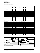
Note 1: “Sample time” is the time between conversions once the address byte has been sent to the converter.
Refer to Figure 5-6.
2: This parameter is periodically sampled and not 100% tested.
3: R
PU
= Pull-up resistor on SDA and SCL.
4: SDA and SCL = V
SS
to V
DD
at 400 kHz.
5: t
ACQ
and t
CONV
are dependent on internal oscillator timing. See Figure 5-5 and Figure 5-6 for relation to
SCL.