
Datasheet


2002-2013 Microchip Technology Inc. DS21732D-page 17
MCP3221
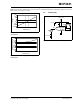
The input signal will initially be sampled with the first
falling edge of the clock following the transmission of a
logic-high R/W bit. Additionally, with the rising edge of
the SCL, the ADC will transmit an acknowledge bit
(ACK = 0). The master must release the data bus dur-
ing this clock pulse to allow the MCP3221 to pull the
line low (refer to Figure 5-3).
For consecutive samples, sampling begins on the fall-
ing edge of the LSB of the conversion result, which is
two bytes long. Refer to Figure 5-6 a for timing diagram.
5.3.2 READING THE CONVERSION DATA
Once the MCP3221 acknowledges the address byte,
the device will transmit four ‘0’ bits followed by the upper
four data bits of the conversion. The master device will
then acknowledge this byte with an ACK = Low. With the
following 8 clock pulses, the MCP3221 will transmit the
lower eight data bits from the conversion. The master
then sends an ACK = high, indicating to the MCP3221
that no more data is requested. The master can then
send a stop bit to end the transmission.
FIGURE 5-5: Executing a Conversion.
5.3.3 CONSECUTIVE CONVERSIONS
For consecutive samples, sampling begins on the fall-
ing edge of the LSB of the conversion result. See
Figure 5-6 for timing.
FIGURE 5-6: Continuous Conversion.
SDA
S
T
A
R
T
S
T
O
P
A
C
K
t
ACQ
+ t
CONV
is
initiated here
Address Byte
Address bits
Device bits
1001
A
R
/
W
Upper Data Byte
0000
D
DD
A
C
K
Lower Data Byte
N
A
K
S P
11
10
2
A
1
A
0
9
D
8
D
7
D
6
D
5
D
4
D
3
D
2
D
1
D
0
12345678910 11 12 13 14 15 16 17 18 19 20 21 22 23 24 25 26 27
SCL
SDA
f
SAMP
= 22.3 ksps (f
CLK
= 400 kHz)
A
C
K
t
ACQ
+ t
CONV
is
initiated here
Address Byte
Address bits
Device bits
1 0 0 1 A2 A1 A0
R
/
W
Upper Data Byte (n)
A
C
K
Lower Data Byte (n)
A
C
K
S
t
ACQ
+ t
CONV
is
initiated here
0000
D
D
D
11
10
9
D
8
D
7
D
6
D
5
D
4
D
3
D
2
D
1
D
0
12345678910 11 12 13 14 15 16 17 18 19 20 21 22 23 24 25 26 27
SCL
S
T
A
R
T
0
28