
Datasheet


MCP19111
DS22331A-page 74 2013 Microchip Technology Inc.
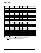
TABLE 11-5: MCP19111 SPECIAL REGISTERS SUMMARY BANK 3
Addr Name Bit 7 Bit 6 Bit 5 Bit 4 Bit 3 Bit 2 Bit 1 Bit 0
Value on
POR Reset
Values on
all other
resets
(1)
Bank 3
180h INDF Addressing this location uses contents of FSR to address data memory (not a physical register) xxxx xxxx uuuu uuuu
181h OPTION_REG
RAPU
INTEDG T0CS T0SE PSA PS2 PS1 PS0
1111 1111 1111 1111
182h PCL Program Counter's (PC) Least Significant byte 0000 0000 0000 0000
183h STATUS
IRP
(2)
RP1
(2)
RP0 TO PD ZDCC
0001 1xxx 000q quuu
184h FSR Indirect data memory address pointer xxxx xxxx uuuu uuuu
185h IOCA IOCA7 IOCA6 IOCA5 IOCA4 IOCA3 IOCA2 IOCA1 IOCA0 0000 0000 0000 0000
186h IOCB IOCB7 IOCB6 IOCB5 IOCB4
— IOCB2 IOCB1 IOCB0 0000 -000 0000 -000
187h ANSELA
— — — — ANSA3 ANSA2 ANSA1 ANSA0 ---- 1111 ---- 1111
188h ANSELB
— — ANSB5 ANSB4 — ANSB2 ANSB1 — --11 -11- --11 -11-
189h — Unimplemented — —
18Ah PCLATH
— — — Write buffer for upper 5 bits of program counter ---0 0000 ---0 0000
18Bh INTCON GIE PEIE T0IE INTE IOCE T0IF INTF IOCF
(4)
0000 000x 0000 000u
18Ch PORTICD
(5)
In-Circuit Debug Port Register
18Dh TRISICD
(5)
In-Circuit Debug TRIS Register
18Eh ICKBUG
(5)
In-Circuit Debug Register 0--- ---- 0--- ----
18Fh BIGBUG
(5)
In-Circuit Debug Breakpoint Register ---- ---- ---- ----
190h PMCON1
— CALSEL — — —WRENWR RD-0-- -000 -0-- -000
191h PMCON2 Program Memory Control Register 2 (not a physical register) ---- ---- ---- ----
192h PMADRL
PMADRL7
PMADRL6 PMADRL5 PMADRL4 PMADRL3 PMADRL2 PMADRL1 PMADRL0
0000 0000 0000 0000
193h PMADRH
— — — — —
PMADRH2 PMADRH1 PMADRH0
---- -000 ---- -000
194h PMDATL
PMDATL7 PMDATL6 PMDATL5 PMDATL4 PMDATL3 PMDATL2 PMDATL1 PMDATL0
0000 0000 0000 0000
195h PMDATH
— —
PMDATH5 PMDATH4 PMDATH3 PMDATH2 PMDATH1 PMDATH0
--00 0000 --00 0000
196h — Unimplemented — —
197h — Unimplemented — —
198h OSCCAL
— FCALT6 FCALT5 FCALT4 FCALT3 FCALT2 FCALT1 FCALT0 xxxx xxxx uuuu uuuu
199h DOVCAL
— — — — DOVT3 DOVT2 DOVT1 DOVT0 xxxx xxxx uuuu uuuu
19Ah TTACAL
— — — — TTA3 TTA2 TTA1 TTA0 xxxx xxxx uuuu uuuu
19Bh BGRCAL Reserve
d
Reserved Reserved Reserved BGRT3 BGRT2 BGRT1 BGRT0 xxxx xxxx uuuu uuuu
19Ch VROCAL
— — — — VROT3 VROT2 VROT1 VROT0 xxxx xxxx uuuu uuuu
19Dh ZROCAL
— — — — ZROT3 ZROT2 ZROT1 ZROT0 xxxx xxxx uuuu uuuu
19Eh — Unimplemented — —
19Fh ATSTCON
— — — — HIDIS LODIS BNCHEN DRVDIS 1--0 0001 1--0 0001
Legend: — = Unimplemented locations read as ‘0’, u = unchanged, x = unknown, q = value depends on condition, shaded = unimplemented
Note 1: Other (non power-up) resets include MCLR
Reset and Watchdog Timer Reset during normal operation.
2: IRP & RP1 bits are reserved, always maintain these bits clear.
3: RA3 pull-up is enabled when pin is configured as MCLR
in Configuration Word.
4: MCLR
and WDT Reset does not affect the previous value data latch. The IOCF bit will be cleared upon reset but will set again if the
mismatch exists.
5: Only accessible when DBGEN
= 0 and ICKBUG<INBUG> = 1.