
Datasheet


2013 Microchip Technology Inc. DS22331A-page 73
MCP19111
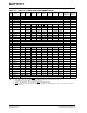
TABLE 11-4: MCP19111 SPECIAL REGISTERS SUMMARY BANK 2
Adr Name Bit 7 Bit 6 Bit 5 Bit 4 Bit 3 Bit 2 Bit 1 Bit 0
Value on
POR Reset
Value on
all other
resets
(1)
Bank 2
100h INDF Addressing this location uses contents of FSR to address data memory (not a physical register) xxxx xxxx xxxx xxxx
101h TMR0 Timer0 Module’s Register xxxx xxxx uuuu uuuu
102h PCL Program Counter's (PC) Least Significant byte 0000 0000 0000 0000
103h STATUS
IRP
(2)
RP1
(2)
RP0 TO PD ZDCC
0001 1xxx 000q quuu
104h FSR Indirect data memory address pointer xxxx xxxx uuuu uuuu
105h WPUGPA
— —
WPUA5
— WPUA3 WPUA2 WPUA1 WPUA0
--1- 1111 --u- uuuu
106h WPUGPB WPUB7 WPUB6
WPUB5 WPUB4
— WPUB2 WPUB1 —
1111 -11- uuuu -uu-
107h PE1 DECON DVRSTR HDLYBY LDLYBY PDEN PUEN UVTEE OVTEE
0000 1100 0000 1100
108h BUFFCON MLTPH2 MLTPH1 MLTPH0 ASEL4 ASEL3 ASEL2 ASEL1 ASEL0
0000 0000 0000 0000
109h ABECON OVDCEN UVDCEN MEASEN SLCPBY CRTMEN TMPSEN RECIREN PATHEN
0000 0000 0000 0000
10Ah PCLATH
— — — Write buffer for upper 5 bits of program counter ---0 0000 ---0 0000
10Bh INTCON GIE PEIE T0IE INTE IOCE T0IF INTF IOCF
(3)
0000 000x 0000 000u
10Ch — Unimplemented — —
10Dh — Unimplemented — —
10Eh
— Unimplemented — —
10Fh
— Unimplemented — —
110h
SSPADD ADD<7:0> 0000 0000 0000 0000
111h SSPBUF Synchronous Serial Port Receive Buffer/Transmit Register xxxx xxxx uuuu uuuu
112h SSPCON1 WCOL SSPOV SSPEN CKP SSPM>3:0> 0000 0000 0000 0000
113h SSPCON2 GCEN ACKSTAT ACKDT ACKEN RCEN PEN RSEN SEN 0000 0000 0000 0000
114h SSPCON3 ACKTIM PCIE SCIE BOEN SDAHT SBCDE AHEN DHEN 0000 0000 0000 0000
115h SSPMSK MSK<7:0> 1111 1111 1111 1111
116h SSPSTAT SMP CKE D/A
PSR/WUA BF — —
117h SSPADD2 ADD2<7:0> 0000 0000 0000 0000
118h SSPMSK2 MSK2<7:0> 1111 1111 1111 1111
119h — Unimplemented — —
11Ah — Unimplemented — —
11Bh — Unimplemented — —
11Ch
— Unimplemented — —
11Dh — Unimplemented — —
11Eh — Unimplemented — —
11Fh — Unimplemented — —
Legend: — = Unimplemented locations read as ‘0’, u = unchanged, x = unknown, q = value depends on condition shaded = unimplemented
Note 1: Other (non power-up) resets include MCLR
Reset and Watchdog Timer Reset during normal operation.
2: IRP & RP1 bits are reserved, always maintain these bits clear.
3: MCLR
and WDT reset does not affect the previous value data latch. The IOCF bit will be cleared upon reset but will set again if the
mismatch exists.