
Datasheet


MCP19111
DS22331A-page 72 2013 Microchip Technology Inc.
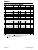
TABLE 11-3: MCP19111 SPECIAL REGISTERS SUMMARY BANK 1
Addr Name Bit 7 Bit 6 Bit 5 Bit 4 Bit 3 Bit 2 Bit 1 Bit 0
Value on
POR Reset
Values on
all other
resets
(1)
Bank 1
80h INDF Addressing this location uses contents of FSR to address data memory (not a physical register) xxxx xxxx uuuu uuuu
81h OPTION_REG
RAPU
INTEDG T0CS T0SE PSA PS2 PS1 PS0
1111 1111 1111 1111
82h PCL Program Counter's (PC) Least Significant byte 0000 0000 0000 0000
83h STATUS
IRP
(2)
RP1
(2)
RP0 TO PD ZDCC
0001 1xxx 000q quuu
84h FSR Indirect data memory address pointer xxxx xxxx uuuu uuuu
85h TRISGPA TRISA7 TRISA6 TRISA5 TRISA4 TRISA3 TRISA2 TRISA1 TRISA0 1111 1111 1111 1111
86h TRISGPB TRISB7 TRISB6 TRISB5 TRISB4
— TRISB2 TRISB1 TRISB0 1111 1111 1111 1111
87h PIE1
— ADIE BCLIE SSPIE — — TMR2IE TMR1IE -000 --00 -000 --00
88h PIE2 UVIE
—OCIEOVIE— — VINIE DCERIE 0-00 --00 0-00 --00
89h APFCON
— — —
— — — — CLKSEL ---- ---0 ---- ---0
8Ah PCLATH
— — — Write buffer for upper 5 bits of program counter ---0 0000 ---0 0000
8Bh INTCON GIE PEIE T0IE INTE IOCE T0IF INTF IOCF
(4)
0000 000x 0000 000u
8Ch — Unimplemented — —
8Dh — Unimplemented — —
8Eh — Unimplemented — —
8Fh — Unimplemented — —
90h VINLVL UVLOEN
— UVLO5 UVLO4 UVLO3 UVLO2 UVLO1 UVLO0
0-xx xxxx 0-uu uuuu
91h OCCON OCEN OCLEB1 OCLEB0 OOC4 OOC3 OOC2 OOC1 OOC0
0xxx xxxx 0uuu uuuu
92h —
— — Reserved Reserved Reserved Reserved Reserved Reserved
--xx xxxx --uu uuuu
93h CSGSCON
— Reserved Reserved Reserved CSGS3 CSGS2 CSGS1 CSGS0
-xxx xxxx -uuu uuuu
94h — Reserved Reserved Reserved Reserved Reserved Reserved Reserved Reserved
xxxx xxxx uuuu uuuu
95h CSDGCON CSDGEN
— — — Reserved CSDG2 CSDG1 CSDG0
0--- xxxx 0--- uuuu
96h —
— — — — Reserved Reserved Reserved Reserved
---- xxxx ---- uuuu
97h VZCCON VZC7 VZC6 VZC5 VZC4 VZC3 VZC2 VZC1 VZC0
xxxx xxxx uuuu uuuu
98h CMPZCON CMPZF3 CMPZF2 CMPZF1 CMPZF0 CMPZG3 CMPZG2 CMPZG1 CMPZG0
xxxx xxxx uuuu uuuu
99h OUVCON OUV7 OUV6 OUV5 OUV4 OUV3 OUV2 OUV1 OUV0
xxxx xxxx uuuu uuuu
9Ah OOVCON OOV7 OOV6 OOV5 OOV4 OOV3 OOV2 OOV1 OOV0
xxxx xxxx uuuu uuuu
9Bh DEADCON HDLY3 HDLY2 HDLY1 HDLY0 LDLY3 LDLY2 LDLY1 LDLY0
xxxx xxxx uuuu uuuu
9Ch SLPCRCON SLPG3 SLPG2 SLPG1 SLPG0 SLPS3 SLPS2 SLPS1 SLPS0
xxxx xxxx uuuu uuuu
9Dh SLVGNCON
— — — SLVGN4 SLVGN3 SLVGN2 SLVGN1 SLVGN0
---x xxxx ---u uuuu
9Eh RELEFF MSDONE RE6 RE5 RE4 RE3 RE2 RE1 RE0
0000 0000 0000 0000
9Fh — Unimplemented — —
Legend: — = Unimplemented locations read as ‘0’, u = unchanged, x = unknown, q = value depends on condition, shaded = unimplemented
Note 1: Other (non power-up) resets include MCLR
Reset and Watchdog Timer Reset during normal operation.
2: IRP & RP1 bits are reserved, always maintain these bits clear.
3: RA3 pull-up is enabled when pin is configured as MCLR
in Configuration Word.
4: MCLR
and WDT Reset does not affect the previous value data latch. The IOCF bit will be cleared upon reset but will set again if the
mismatch exists.