
Datasheet


2013 Microchip Technology Inc. DS22331A-page 71
MCP19111
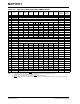
TABLE 11-2: MCP19111 SPECIAL REGISTERS SUMMARY BANK 0
Adr Name Bit 7 Bit 6 Bit 5 Bit 4 Bit 3 Bit 2 Bit 1 Bit 0
Value on
POR Reset
Value on
all other
resets
(1)
Bank 0
00h INDF Addressing this location uses contents of FSR to address data memory (not a physical register) xxxx xxxx xxxx xxxx
01h TMR0 Timer0 Module’s Register xxxx xxxx uuuu uuuu
02h PCL Program Counter's (PC) Least Significant byte 0000 0000 0000 0000
03h STATUS
IRP RP1 RP0 TO
PD ZDCC
0001 1xxx 000q quuu
04h FSR Indirect data memory address pointer xxxx xxxx uuuu uuuu
05h PORTGPA GPA7 GPA6
GPA5 GPA4 GPA3 GPA2 GPA1 GPA0
xxxx xxxx uuuu uuuu
06h PORTGPB GPB7 GPB6 GPB5 GPB4
— GPB2 GPB1 GPB0 xxx- xxxx uuu- uuuu
07h PIR1
— ADIF BCLIF SSPIF — —TMR2IFTMR1IF-000 --00 -000 --00
08h PIR2 UVIF
—OCIFOVIF— — VINIF DCERIF 0-00 --00 0-00 --00
09h PCON
— —
— —
—OTPOR —
---- -qq- ---- -uu-
0Ah PCLATH
— — — Write buffer for upper 5 bits of program counter ---0 0000 ---0 0000
0Bh INTCON GIE PEIE T0IE INTE IOCE T0IF INTF IOCF
(3)
0000 000x 0000 000u
0Ch TMR1L Holding register for the Least Significant byte of the 16-bit TMR1 xxxx xxxx uuuu uuuu
0Dh
TMR1H Holding register for the Most Significant byte of the 16-bit TMR1 xxxx xxxx
uuuu uuuu
0Eh
T1CON
— — T1CKPS1 T1CKPS0 — — TMR1CS TMR1ON --00 --00
--uu --uu
0Fh
TMR2 Timer2 Module Register
0000 0000
uuuu uuuu
10h
T2CON — — — — — TMR2ON T2CKPS1 T2CKPS0
---- -000
---- -000
11h PR2 Timer2 Module Period Register
1111 1111
1111 1111
12h — Unimplemented
—
—
13h PWMPHL SLAVE Phase Shift Register
xxxx xxxx uuuu uuuu
14h PWMPHH SLAVE Phase Shift Register
xxxx xxxx uuuu uuuu
15h PWMRL PWM Register Low Byte
xxxx xxxx uuuu uuuu
16h PWMRH PWM Register High Byte
xxxx xxxx uuuu uuuu
17h — Unimplemented
— —
18h — Unimplemented
— —
19h OVCCON OVC7 OVC6 OVC5 OVC4 OVC3 OVC2 OVC1 OVC0 0000 0000 0000 0000
1Ah OVFCON VOUTON
— — OVF4 OVF3 OVF2 OVF1 OVF0
0--0 0000 0--0 0000
1Bh OSCTUNE
— — — TUN4 TUN3 TUN2 TUN1 TUN0 ---0 0000 ---0 0000
1Ch
ADRESL Least significant 8 bits of the right-shifted result xxxx xxxx uuuu uuuu
1Dh
ADRESH Most significant 2 bits of right-shifted result ---- --xx uuuu uuuu
1Eh ADCON0
— CHS4
CHS3
CHS2 CHS1 CHS0 GO/DONE ADON -000 0000 -000 0000
1Fh ADCON1
— ADCS2 ADCS1 ADCS0 — — — — -000 ---- -000 ----
Legend: — = Unimplemented locations read as ‘0’, u = unchanged, x = unknown, q = value depends on condition shaded = unimplemented
Note 1: Other (non power-up) resets include MCLR
Reset and Watchdog Timer Reset during normal operation.
2: IRP & RP1 bits are reserved, always maintain these bits clear.
3: MCLR
and WDT reset does not affect the previous value data latch. The IOCF bit will be cleared upon reset but will set again if the
mismatch exists.