
Datasheet


MCP19111
DS22331A-page 142 2013 Microchip Technology Inc.
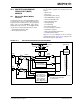
FIGURE 26-1: SIMPLIFIED PWM BLOCK DIAGRAM
A PWM output (Figure 26-2) has a time base (period)
and a time that the output stays high (duty cycle). The
frequency of the PWM is the inverse of the period
(1/period).
FIGURE 26-2: PWM OUTPUT
26.1.3 PWM PERIOD
The PWM period is specified by writing to the PR2
register. The PWM period can be calculated using the
following equation:
EQUATION 26-3:
When TMR2 is equal to PR2, the following two events
occur on the next increment cycle:
•TMR2 is cleared
• The PWM duty cycle is latched from PWMRL into
PWMRH
CLKPIN_IN
R
SQ
Q
OSC
SYSTEM
CLOCK
LATCH DATA
LATCH DATA
RESET TIMER
8 8
8
8
Comparator Comparator
Comparator
TMR2
(Note 1)
88
8
8
PR2
PWMPHL
PWMRL
PWMRH
(SLAVE)
PWMPHH
(SLAVE)
Note 1: TIMER 2 should be clocked by F
OSC
(8 MHz).
Period
Duty Cycle
TMR2 = PR2 + 1
TMR2 = PWMRH
TMR2 = PR2 + 1
PWM PERIOD=[(PR2)+1] x T
OSC
x(T2 PRESCALE VALUE)