
Datasheet


2013 Microchip Technology Inc. DS22331A-page 141
MCP19111
26.0 PWM MODULE
The CCP module implemented on the MCP19111 is a
modified version of the CCP module found in standard
mid-range microcontrollers. In the MCP19111, the
PWM module is used to generate the system clock or
system oscillator. This system clock will control the
MCP19111 switching frequency, as well as set the
maximum allowable duty cycle. The PWM module
does not continuously adjust the duty cycle to control
the output voltage. This is accomplished by the analog
control loop and associated circuitry.
26.1 Standard Pulse-Width Modulation
(PWM) Mode
The PWM module output signal is used to set the
operating switching frequency and maximum
allowable duty cycle of the MCP19111. The actual duty
cycle on the HDRV and LDRV is controlled by the
analog PWM control loop. However, this duty cycle
cannot be greater than the value in the PWMRL
register.
There are two modes of operation that concern the
system clock PWM signal. These modes are
stand-alone (non-frequency synchronization) and
frequency synchronization.
26.1.1 STAND-ALONE (NON-FREQUENCY
SYNCHRONIZATION) MODE
When the MCP19111 is running stand-alone, the PWM
signal functions as the system clock. It is operating at
the programmed switching frequency with a
programmed maximum duty cycle (D
CLOCK
). The
programmed maximum duty cycle is not adjusted on a
cycle-by-cycle basis to control the MCP19111 system
output. The required duty cycle (D
BUCK
) to control the
output is adjusted by the MCP19111 analog control
loop and associated circuitry. D
CLOCK
does, however,
set the maximum allowable D
BUCK
.
EQUATION 26-1:
26.1.2 SWITCHING FREQUENCY
SYNCHRONIZATION MODE
The MCP19111 can be programmed to be a switching
frequency MASTER or SLAVE device. The MASTER
device functions as described in Section 26.1.1
“Stand-Alone (Non-Frequency Synchronization)
Mode” with the exception of the system clock also
being applied to GPA1.
A SLAVE device will receive the MASTER system
clock on GPA1. This MASTER system clock will be
OR’ed with the output of the TIMER2 module. This
OR’ed signal will latch PWMRL into PWMRH and
PWMPHL into PWMPHH.
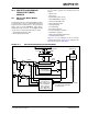
Figure 26-1 shows a simplified block diagram of the
CCP module in PWM mode.
The PWMPHL register allows for a phase shift to be
added to the SLAVE system clock.
It is desired to have the MCP19111 SLAVE devices
system clock start point shifted by a programmed
amount from the MASTER system clock. This SLAVE
phase shift is specified by writing to the PWMPHL reg-
ister. The SLAVE phase shift can be calculated by
using the following equation.
EQUATION 26-2:
D
BUCK
1D
CLOCK
–
SLAVE PHASE SHIFT=PWMPHL•TOSC•(T2 PRESCALE VALUE)