
Datasheet


2013 Microchip Technology Inc. DS22331A-page 135
MCP19111
24.0 TIMER1 MODULE WITH GATE
CONTROL
The Timer1 module is a 16-bit timer with the following
features:
• 16-bit timer register pair (TMR1H:TMR1L)
• Readable and Writable (both registers)
• Selectable internal clock source
• 2-bit prescaler
• Interrupt on overflow
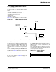
Figure 24-1 is a block diagram of the Timer1 module.
FIGURE 24-1: TIMER1 BLOCK DIAGRAM
24.1 Timer1 Operation
The Timer1 module is a 16-bit incrementing timer which
is accessed through the TMR1H:TMR1L register pair.
Writes to TMR1H or TMR1L directly update the
counter. The timer is incremented on every instruction
cycle.
Timer1 is enabled by configuring the TMR1ON bit in the
T1CON register. Table 24-1 displays the Timer1 enable
selections.
24.2 Clock Source Selection
The TMR1CS bit of the T1CON register is used to select
the clock source for Timer1. Table 24-1 displays the
clock source selections.
24.2.1 INTERNAL CLOCK SOURCE
The TMR1H:TMR1L register pair will increment on
multiples of F
OSC
or F
OSC
/4 as determined by the
Timer1 prescaler.
As an example, when the F
OSC
internal clock source is
selected, the Timer1 register value will increment by four
counts every instruction clock cycle.
TMR1H
TMR1L
TMR1CS
T1CKPS<1:0>
Prescaler
1, 2, 4, 8
1
0
2
Set flag bit
TMR1IF on
Overflow
TMR1
(1)
TMR1ON
Note 1: TMR1 register increments on rising edge.
F
OSC
F
OSC
/4
TABLE 24-1: CLOCK SOURCE
SELECTIONS
TMR1CS Clock Source
1 8 MHz system Clock (F
OSC
)
0 2 MHz instruction clock (F
OSC
/4)