
Datasheet


MCP19111
DS22331A-page 126 2013 Microchip Technology Inc.
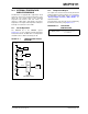
22.2 ADC Operation
22.2.1 STARTING A CONVERSION
To enable the ADC module, the ADON bit of the
ADCON0 register must be set to a ‘1’. Setting the
GO/DONE bit of the ADCON0 register to a ‘1’ will start
the Analog-to-Digital conversion.
22.2.2 COMPLETION OF A CONVERSION
When the conversion is complete, the ADC module will:
• Clear the GO/DONE
bit
• Set the ADIF Interrupt Flag bit
• Update the ADRESH:ADRESL registers with new
conversion result
22.2.3 TERMINATING A CONVERSION
If a conversion must be terminated before completion,
the GO/DONE
bit can be cleared in software. The
ADRESH:ADRESL registers will not be updated with
the partially complete Analog-to-Digital conversion
sample. Instead, the ADRESH:ADRESL register pair
will retain the value of the previous conversion.
Additionally, a two T
AD
delay is required before another
acquisition can be initiated. Following the delay, an
input acquisition is automatically started on the
selected channel.
22.2.4 ADC OPERATION DURING SLEEP
The ADC module can operate during Sleep. This
requires the ADC clock source to be set to the F
RC
option. When the F
RC
clock source is selected, the
ADC waits one additional instruction before starting the
conversion. This allows the SLEEP instruction to be
executed, which can reduce system noise during the
conversion. If the ADC interrupt is enabled, the device
will wake-up from Sleep when the conversion
completes. If the ADC interrupt is disabled, the ADC
module is turned off after the conversion completes,
although the ADON bit remains set.
When the ADC clock source is something other than
F
RC
, a SLEEP instruction causes the present
conversion to be aborted and the ADC module is
turned off, although the ADON bit remains set.
22.2.5 A/D CONVERSION PROCEDURE
This is an example procedure for using the ADC to
perform an Analog-to-Digital conversion:
1. Configure Port:
• Disable pin output driver (Refer to the TRIS
register)
• Configure pin as analog (Refer to the ANSEL
register)
2. Configure the ADC module:
• Select ADC conversion clock
• Select ADC input channel
• Turn on ADC module
3. Configure ADC interrupt (optional):
• Clear ADC interrupt flag
• Enable ADC interrupt
• Enable peripheral interrupt
• Enable global interrupt
(1)
4. Wait the required acquisition time
(2)
.
5. Start conversion by setting the GO/DONE
bit.
6. Wait for ADC conversion to complete by one of
the following:
• Polling the GO/DONE
bit
• Waiting for the ADC interrupt (interrupts
enabled)
7. Read ADC Result.
8. Clear the ADC interrupt flag (required if interrupt
is enabled).
EXAMPLE 22-1: A/D CONVERSION
Note: The GO/DONE bit should not be set in the
same instruction that turns on the ADC.
Refer to Section 22.2.5 “A/D
Conversion Procedure”.
Note: A device Reset forces all registers to their
Reset state. Thus, the ADC module is
turned off and any pending conversion is
terminated.
Note 1: The global interrupt can be disabled if the
user is attempting to wake-up from Sleep
and resume in-line code execution.
2: Refer to Section 22.4 “A/D Acquisition
Requirements”.
;This code block configures the ADC
;for polling, Frc clock and AN0 input.
;
;Conversion start & polling for completion ;
are included.
;
BANKSEL ADCON1 ;
MOVLW B’01110000’ ;Frc clock
MOVWF ADCON1 ;
BANKSEL TRISGPA ;
BSF TRISGPA,0 ;Set GPA0 to input
BANKSEL ANSELA ;
BSF ANSELA,0 ;Set GPA0 to analog
BANKSEL ADCON0 ;
MOVLW B’01000001’ ;Select channel AN0
MOVWF ADCON0 ;Turn ADC On
CALL SampleTime ;Acquisiton delay
BSF ADCON0,1 ;Start conversion
BTFSC ADCON0,1 ;Is conversion done?
GOTO $-1 ;No, test again
BANKSEL ADRESH ;
MOVF ADRESH,W ;Read upper 2 bits
MOVWF RESULTHI ;store in GPR space
BANKSEL ADRESL ;
MOVF ADRESL,W ;Read lower 8 bits
MOVWF RESULTLO ;Store in GPR space