
Datasheet


2013 Microchip Technology Inc. DS22331A-page 125
MCP19111
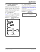
FIGURE 22-2: ANALOG-TO-DIGITAL CONVERSION T
AD
CYCLES
22.1.4 INTERRUPTS
The ADC module allows for the ability to generate an
interrupt upon completion of an Analog-to-Digital
conversion. The ADC Interrupt Flag is the ADIF bit in
the PIR1 register. The ADC Interrupt Enable is the
ADIE bit in the PIE1 register. The ADIF bit must be
cleared in software.
This interrupt can be generated while the device is
operating, or while in Sleep. If the device is in Sleep,
the interrupt will wake-up the device. Upon waking from
Sleep, the next instruction following the SLEEP
instruction is always executed. If the user is attempting
to wake-up from Sleep and resume in-line code
execution, the GIE and PEIE bits of the INTCON
register must be disabled. If the GIE and PEIE bits of
the INTCON register are enabled, execution will switch
to the Interrupt Service Routine.
22.1.5 RESULT FORMATTING
The 10-bit A/D conversion result is supplied in right jus-
tified format only.
Figure 22-3 shows the output format.
FIGURE 22-3: 10-BIT A/D RESULT FORMAT
T
AD
1
T
AD
2
T
AD
3 T
AD
4
T
AD
5 T
AD
6
T
AD
7
T
AD
8 T
AD
11
Set GO/DONE bit
Holding capacitor is disconnected from analog input (typically 100 ns)
T
AD
9
T
AD
10T
CY
- T
AD
ADRESH:ADRESL is loaded, GO bit is cleared,
ADIF bit is set, holding capacitor is connected to analog input.
Conversion starts
b0
b9
b6
b5
b4
b3
b2
b1
b8
b7
On the following cycle:
Note 1: The ADIF bit is set at the completion of
every conversion, regardless of whether
or not the ADC interrupt is enabled.
2: The ADC operates during Sleep-only
when the F
RC
oscillator is selected.
(ADFM = 1) MSB LSB
bit 7 bit 0 bit 7 bit 0
Read as ‘0’ 10-bit A/D Result