
Datasheet


MCP19111
DS22331A-page 124 2013 Microchip Technology Inc.
22.1 ADC Configuration
When configuring and using the ADC, the following
functions must be considered:
• Port configuration
• Channel selection
• ADC conversion clock source
• Interrupt control
• Result formatting
22.1.1 PORT CONFIGURATION
The ADC can be used to convert both analog and
digital signals. When converting analog signals, the I/O
pin should be configured for analog by setting the
associated TRIS and ANSEL bits. Refer to
Section 19.0 “I/O Ports” for more information.
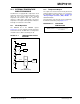
22.1.2 CHANNEL SELECTION
There are up to 21 channel selections available:
• AN<6:0> pins
• VIN: 1/5 of the input voltage (V
IN
)
•VREGREF: V
OUT
reference voltage
• OV_REF: reference for OV comparator
• UV_REF: reference for UV comparator
• VBGR: band gap reference
• VOUT: output voltage
• CRT: voltage proportional to the AC inductor
current
• VZC: an internal ground, Voltage for Zero Current
• DEMAND: input to slope compensation circuitry
• RELEFF: relative efficient measurement channel
• TMP_ANA: voltage proportional to silicon die tem-
perature
• ANA_IN: for a multi-phase slave, error amplifier
signal received from master
• DCI: DC inductor valley current
The CHS<4:0> bits of the ADCON0 register determine
which channel is connected to the sample and hold
circuit.
When changing channels, a delay is required before
starting the next conversion. Refer to Section 22.2
“ADC Operation” for more information.
22.1.3 ADC CONVERSION CLOCK
The source of the conversion clock is software
selectable via the ADCS bits of the ADCON1 register.
There are five possible clock options:
•F
OSC
/8
•F
OSC
/16
•F
OSC
/32
•F
OSC
/64
•F
RC
(clock derived from internal oscillator with a
divisor of 16)
The time to complete one bit conversion is defined as
T
AD
. One full 10-bit conversion requires 11 T
AD
periods
as shown in Figure 22-2.
For a correct conversion, the appropriate T
AD
specification must be met. Refer to the A/D conversion
requirements in Section 5.0 “Digital Electrical
Characteristics” for more information. Table 22-1
gives examples of appropriate ADC clock selections.
Note: Analog voltages on any pin that is defined
as a digital input may cause the input
buffer to conduct excess current.
Note: Unless using the F
RC
, any changes in the
system clock frequency will change the
ADC clock frequency, which may
adversely affect the ADC result.
TABLE 22-1: ADC CLOCK PERIOD (T
AD
) VS.
DEVICE OPERATING
FREQUENCIES
ADC Clock Period (T
AD
)
Device
Frequency
(F
OSC
)
ADC
Clock Source
ADCS<2:0> 8 MHz
F
OSC
/8 001 1.0 µs
(2)
F
OSC
/16 101 2.0 µs
F
OSC
/32 010 4.0 µs
F
OSC
/64 110 8.0 µs
(3)
F
RC
x11 2.0 – 6.0 µs
(1,4)
Legend: Shaded cells are outside of recommended
range.
Note 1: The F
RC
source has a typical T
AD
time of
4µs for V
DD
>3.0V.
2: These values violate the minimum
required T
AD
time.
3: For faster conversion times, the selection
of another clock source is recommended.
4: The F
RC
clock source is only
recommended if the conversion will be
preformed during Sleep.