
Datasheet


2013 Microchip Technology Inc. DS22331A-page 123
MCP19111
22.0 ANALOG-TO-DIGITAL
CONVERTER (ADC) MODULE
The Analog-to-Digital Converter (ADC) allows
conversion of an analog input signal to a 10-bit binary
representation of that signal. This device uses analog
inputs, which are multiplexed into a single sample and
hold circuit. The output of the sample and hold is
connected to the input of the converter. The converter
generates a 10-bit binary result via successive
approximation and stores the right justified conversion
result into the ADC result registers (ADRESH:ADRESL
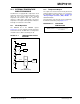
register pair). Figure 22-1 shows the block diagram of
the ADC.
The internal band gap supplies the voltage reference to
the ADC.
The ADC can generate an interrupt upon completion of
a conversion. This interrupt can be used to wake-up the
device from Sleep.
FIGURE 22-1: ADC BLOCK DIAGRAM
Note 1: When ADON = 0, all multiplexer inputs are disconnected.
2: See ADCON0 register (Register 22-1) for detailed analog channel selection per device.
00000
00001
00010
00011
00100
00101
00111
00110
01000
01001
01010
01011
RELEFF
ADC
V
OUT
V
REF
ADON
GO/DONE
CHS4:CHS0
ADRESH ADRESL
10
V
SS
TEMP_ANA
GPA0
V
IN_ANA
CRT
GPB4
VZC
V
REF
OV
REF
UV
REF
V
BGR
ANA_IN
DEMAND
GPB2
DCI
01100
GPA1
GPA3
GPA2
GPB1
GPB5
10000
10001
10010
10011
10100
10101
10110
10111