
Datasheet


2013 Microchip Technology Inc. DS22331A-page 107
MCP19111
18.3.2 WRITING TO THE FLASH
PROGRAM MEMORY
A word of the Flash program memory may only be
written to if the word is in an unprotected segment of
memory, as defined in Section 12.1 “Configuration
Word” (bits WRT1:WRT0).
Flash program memory must be written in four-word
blocks. See Figures 18-2 and 18-3 for more details. A
block consists of four words with sequential addresses,
with a lower boundary defined by an address, where
PMADRL<1:0> = 00. All block writes to program
memory are done as 16-word erase by four-word write
operations. The write operation is edge-aligned and
cannot occur across boundaries.
To write program data, it must first be loaded into the
buffer registers (see Figure 18-2). This is accomplished
by first writing the destination address to PMADRL and
PMADRH, and then writing the data to PMDATL and
PMDATH. After the address and data have been set,
then the following sequence of events must be
executed:
1. Write 55h, then AAh, to PMCON2 (Flash
programming sequence).
2. Set the WR control bit of the PMCON1 register.
All four buffer register locations should be written to
with correct data. If less than four words are being writ-
ten to in the block of four words, then a read from the
program memory location(s) not being written to must
be performed. This takes the data from the program
location(s) not being written and loads it into the
PMDATL and PMDATH registers. Then the sequence
of events to transfer data to the buffer registers must be
executed.
To transfer data from the buffer registers to the program
memory, the PMADRL and PMADRH must point to the
last location in the four-word block
(PMADRL<1:0> = 11). Then the following sequence of
events must be executed:
1. Write 55h, then AAh, to PMCON2 (Flash
programming sequence).
2. Set control bit WR of the PMCON1 register to
begin the write operation.
The user must follow the same specific sequence to
initiate the write for each word in the program block,
writing each program word in sequence (000, 001,
010, 011). When the write is performed on the last
word (PMADRL<1:0> = 11), a block of sixteen words is
automatically erased and the content of the four-word
buffer registers are written into the program memory.
After the “BSF PMCON1,WR” instruction, the processor
requires two cycles to set up the erase/write operation.
The user must place two NOP instructions after the WR
bit is set. Since data is being written to buffer registers,
the writing of the first three words of the block appears
to occur immediately. The processor will halt internal
operations for the typical 4 ms, only during the cycle in
which the erase takes place (i.e., the last word of the
sixteen-word block erase). This is not Sleep mode, as
the clocks and peripherals will continue to run. After
the four-word write cycle, the processor will resume
operation with the third instruction after the PMCON1
write instruction. The above sequence must be
repeated for the higher 12 words.
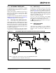
Refer to Figure 18-2 for a block diagram of the buffer
registers and the control signals for test mode.
18.3.3 PROTECTION AGAINST SPURIOUS
WRITE
There are conditions when the device should not write
to the program memory. To protect against spurious
writes, various mechanisms have been built in. On
power-up, WREN is cleared. Also, the Power-up Timer
(72 ms duration) prevents program memory writes.
The write initiate sequence, and the WREN bit, help
prevent an accidental write during a power glitch or
software malfunction.
18.3.4 OPERATION DURING CODE PROTECT
When the device is code protected, the CPU is able to
read and write unscrambled data to the program
memory. The test mode access is disabled.
18.3.5 OPERATION DURING WRITE PROTECT
When the program memory is write protected, the
CPU can read and execute from the program memory.
The portions of program memory that are write pro-
tected can not be modified by the CPU using the
PMCON registers. The write protection has no effect in
ICSP mode.
Note: The write protect bits are used to protect the
users’ program from modification by the
user’s code. They have no effect when
programming is performed by ICSP. The
code-protect bits, when programmed for
code protection, will prevent the program
memory from being written via the ICSP
interface.
Note: An erase is only initiated for the write of four
words, just after a row boundary; or
PMCON1<WR> set with PMADRL<3:0> =
xxxx0011.