
Datasheet


MCP19111
DS22331A-page 106 2013 Microchip Technology Inc.
18.3.1 READING THE FLASH PROGRAM
MEMORY
To read a program memory location, the user must
write two bytes of the address to the PMADRL and
PMADRH registers, and then set control bit RD
(PMCON1<0>). Once the read control bit is set, the
program memory Flash controller will use the second
instruction cycle after to read the data. This causes the
second instruction immediately following the “BSF
PMCON1,RD” instruction to be ignored. The data is
available, in the very next cycle, in the PMDATL and
PMDATH registers; it can be read as two bytes in the
following instructions. PMDATL and PMDATH regis-
ters will hold this value until another read or until it is
written to by the user (during a write operation).
EXAMPLE 18-1: FLASH PROGRAM READ
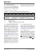
FIGURE 18-1: FLASH PROGRAM MEMORY READ CYCLE EXECUTION – NORMAL MODE
BANKSELPM_ADR; Change STATUS bits RP1:0 to select bank with PMADR
MOVLWMS_PROG_PM_ADDR;
MOVWFPMADRH; MS Byte of Program Address to read
MOVLWLS_PROG_PM_ADDR;
MOVWFPMADRL; LS Byte of Program Address to read
BANKSELPMCON1; Bank to containing PMCON1
BSF PMCON1, RD; EE Read
NOP ; First instruction after BSF PMCON1,RD executes normally
NOP ; Any instructions here are ignored as program
; memory is read in second cycle after BSF PMCON1,RD
;
BANKSELPMDATL; Bank to containing PMADRL
MOVFPMDATL, W; W = LS Byte of Program PMDATL
MOVFPMDATH, W; W = MS Byte of Program PMDATL
Q1 Q2 Q3 Q4 Q1 Q2 Q3 Q4 Q1 Q2 Q3 Q4 Q1 Q2 Q3 Q4 Q1 Q2 Q3 Q4 Q1 Q2 Q3 Q4
BSF PMCON1,RD
Executed here
INSTR (PC + 1)
Executed here
NOP
Executed here
PC PC + 1
PMADRH,PMADRL
PC+3 PC + 5
Flash ADDR
RD bit
INSTR (PC)
PMDATH,PMDATL
INSTR (PC + 3)
PC + 3 PC + 4
INSTR (PC + 4)
INSTR (PC + 1)
INSTR (PC - 1)
Executed here
INSTR (PC + 3)
Executed here
INSTR (PC + 4)
Executed here
Flash DATA
PMDATH
PMDATL
Register
EERHLT