
Datasheet


Table Of Contents
© 2007 Microchip Technology Inc. DS21936C-page 7
MCP1726
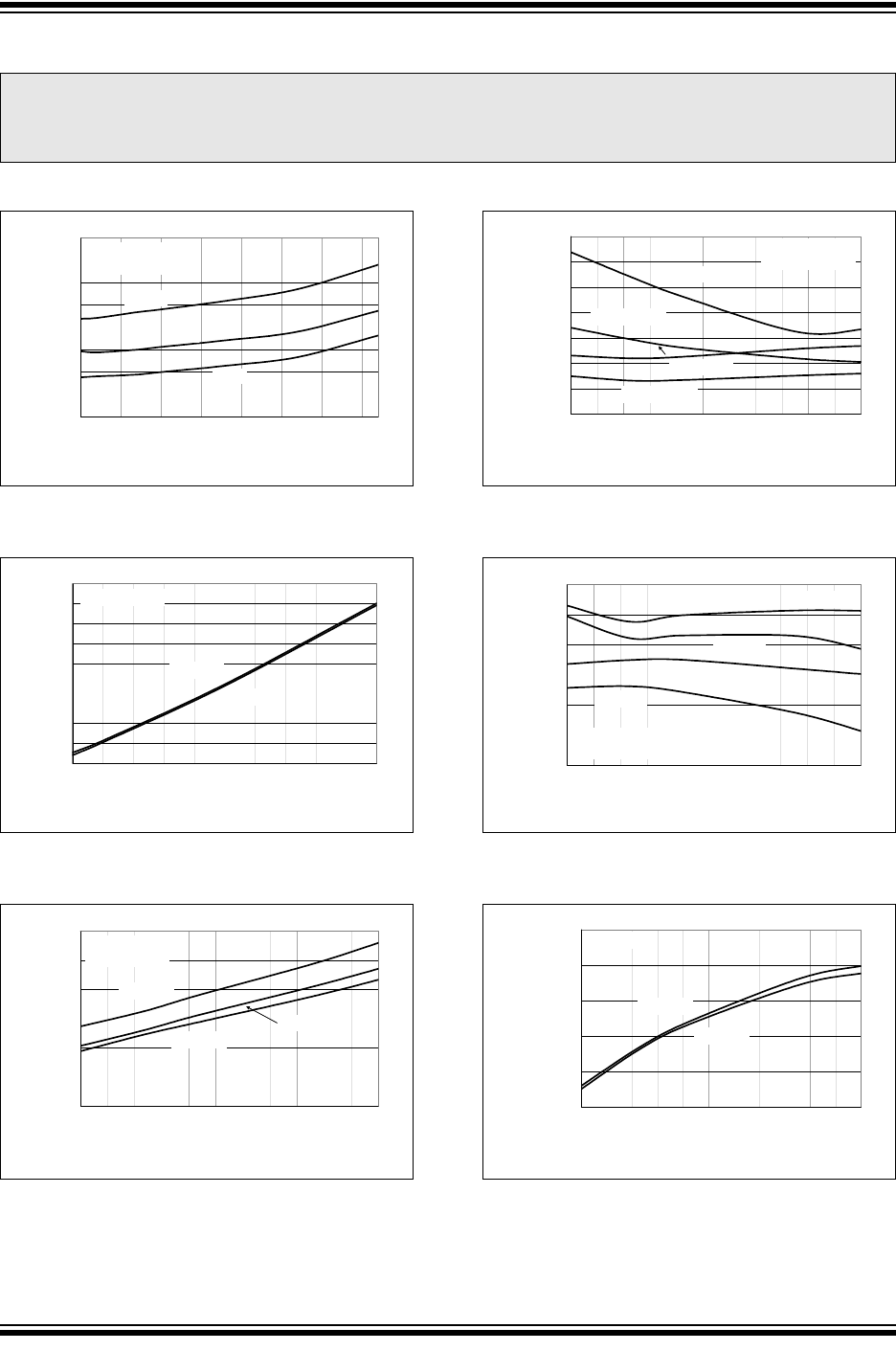
2.0 TYPICAL PERFORMANCE CURVES
NOTE: Unless otherwise indicated, V
IN
= V
OUT
+ 0.5V, I
OUT
= 1 mA and T
A
= +25°C.
FIGURE 2-1: Quiescent Current vs. Input
Voltage (1.2V Adjustable).
FIGURE 2-2: Ground Current vs. Load
Current (1.2V Adjustable).
FIGURE 2-3: Quiescent Current vs.
Junction Temperature (1.2V Adjustable).
FIGURE 2-4: Line Regulation vs.
Temperature (1.2V Adjustable).
FIGURE 2-5: Load Regulation vs.
Temperature.
FIGURE 2-6: Adjust Pin Voltage vs.
Temperature.
Note: The graphs and tables provided following this note are a statistical summary based on a limited number of
samples and are provided for informational purposes only. The performance characteristics listed herein
are not tested or guaranteed. In some graphs or tables, the data presented may be outside the specified
operating range (e.g., outside specified power supply range) and therefore outside the warranted range.
100
110
120
130
140
150
160
170
180
2.32.83.33.84.34.85.35.8
Input Voltage (V)
Quiescent Current (µA)
-40ºC
+125°C
+25°C
V
R
= 1.2V (Adj.)
I
OUT
= 0 mA
120
140
160
180
200
220
240
260
280
300
0 200 400 600 800 1000
Load Current (mA)
Ground Current (µA)
V
IN
= 2.5V
V
IN
= 3.3V
V
R
= 1.2V (Adj.)
100
110
120
130
140
150
160
-40
-25
-10
5
20
35
50
65
80
95
110
125
Temperature (°C)
Quiescent Current (µA)
V
IN
= 2.5V
V
IN
= 5.0V
V
IN
= 3.3V
V
R
= 1.2V (Adj.)
I
OUT
= 0 mA
-0.02
-0.01
0
0.01
0.02
0.03
0.04
0.05
-40
-25
-10
5
20
35
50
65
80
95
110
125
Temperature (°C)
Line Regulation (%/V)
I
OUT
= 1A
I
OUT
= 500 mA
I
OUT
= 100 mA
I
OUT
= 1 mA
V
R
= 1.2V (Adj.)
V
IN
= 2.3V to 6.0V
0.10
0.20
0.30
0.40
0.50
0.60
0.70
-40
-25
-10
5
20
35
50
65
80
95
110
125
Temperature (°C)
Load Regulation (%)
V
R
= 0.8V
V
R
= 1.8V
V
R
= 3.3V
V
R
= 5.0V
V
IN
= V
R
+ 0.6V (or 2.3V)
I
OUT
= 1 mA to 1A
408.50
409.00
409.50
410.00
410.50
411.00
-40
-25
-10
5
20
35
50
65
80
95
110
125
Temperature (°C)
Adjust Pin Voltage (mV)
V
IN
= 6.0V
V
IN
= 2.3V
I
OUT
= 1 mA