
Datasheet


Table Of Contents
MCP1726
DS21936C-page 18 © 2007 Microchip Technology Inc.
5.0 APPLICATION CIRCUITS/
ISSUES
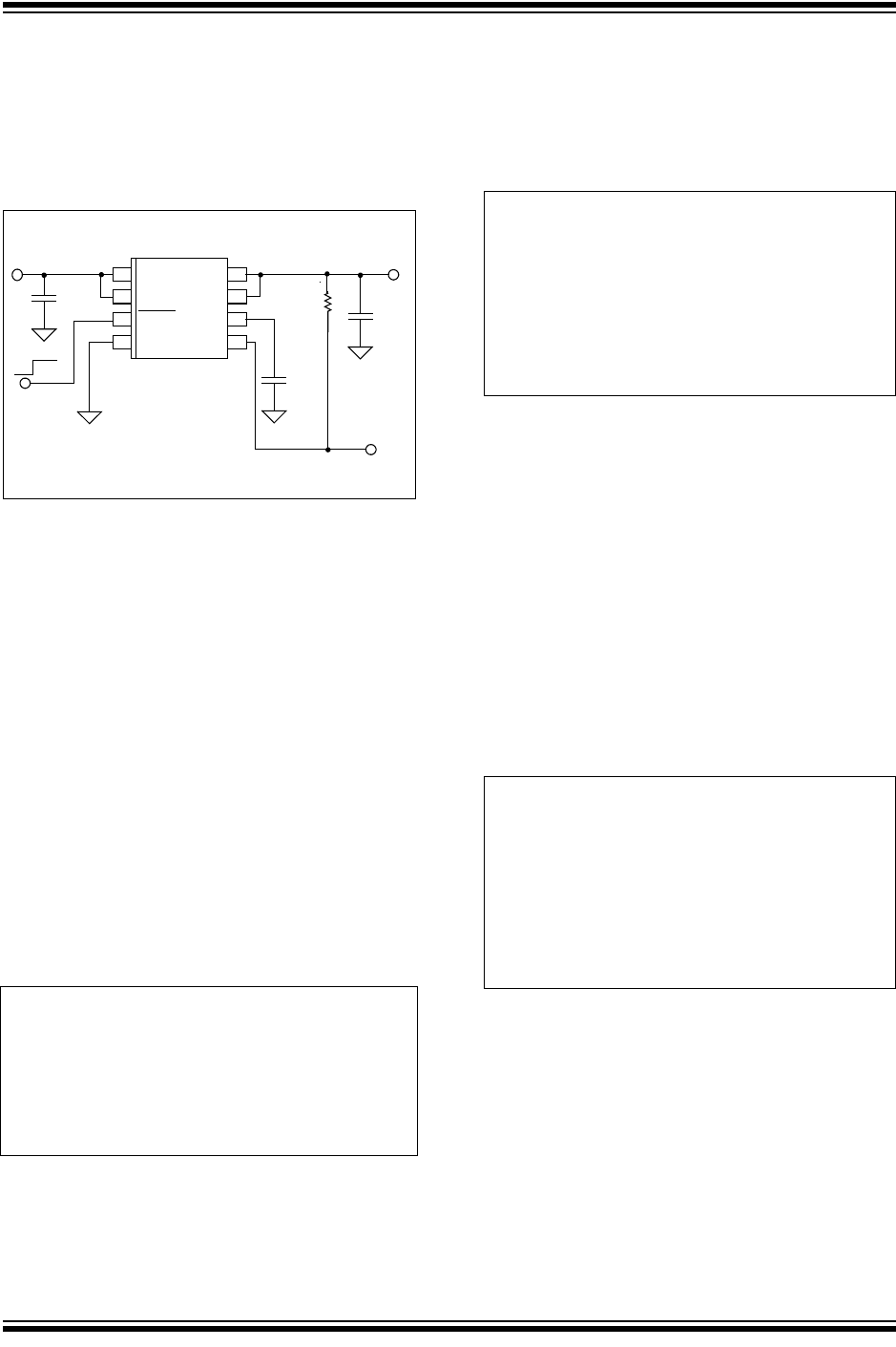
5.1 Typical Application
The MCP1726 is used for applications that require high
LDO output current and a power good output.
FIGURE 5-1: Typical Application Circuit.
5.1.1 APPLICATION CONDITIONS
5.2 Power Calculations
5.2.1 POWER DISSIPATION
The internal power dissipation within the MCP1726 is a
function of input voltage, output voltage, output current
and quiescent current. The following equation can be
used to calculate the internal power dissipation for the
LDO.
EQUATION 5-1:
In addition to the LDO pass element power dissipation,
there is power dissipation within the MCP1726 as a
result of quiescent or ground current. The power dissi-
pation as a result of the ground current can be
calculated using the following equation:
EQUATION 5-2:
The total power dissipated within the MCP1726 is the
sum of the power dissipated in the LDO pass device
and the P(I
GND
) term. Because of the CMOS construc-
tion, the typical I
GND
for the MCP1726 is 140 µA.
Operating at a maximum of 3.63V results in a power
dissipation of 0.51 milli-Watts. For most applications,
this is small compared to the LDO pass device power
dissipation and can be neglected.
The maximum continuous operating junction tempera-
ture specified for the MCP1726 is +125
°C. To estimate
the internal junction temperature of the MCP1726, the
total internal power dissipation is multiplied by the ther-
mal resistance from junction to ambient (Rθ
JA
) of the
device. The thermal resistance from junction to ambi-
ent for the 3x3DFN package is estimated at 41
° C/W.
EQUATION 5-3:
Package Type = 3x3DFN8
Input Voltage Range = 3.3V ± 10%
V
IN
maximum = 3.63V
V
IN
minimum = 2.97V
V
OUT
typical = 2.5V
I
OUT
= 1.0A maximum
V
IN
SHDN
GND
PWRGD
C
DELAY
V
OUT
V
OUT
1
2
3
4
5
6
7
8
10 µF
V
OUT
= 2.5V @ 1A
10 µF
V
IN
= 3.3V
On
Off
V
IN
R
1
C
1
C
2
1000 pF
C
3
MCP1726-2.5
10kΩ
PWRGD
P
LDO
V
IN MAX )()
V
OUT MIN()
–()I
OUT MAX)()
×=
P
LDO
= LDO Pass device internal power
dissipation
V
IN(MAX)
= Maximum input voltage
V
OUT(MIN)
= LDO minimum output voltage
P
IGND()
V
IN MAX()
I
VIN
×=
P
I(GND)
= Power dissipation due to the
quiescent current of the LDO
V
IN(MAX)
= Maximum input voltage
I
VIN
= Current flowing in the V
IN
pin with no
LDO output current (LDO quiescent
current)
T
JMAX()
P
TOTAL
Rθ
JA
× T
AMAX
+=
T
J(MAX)
= Maximum continuous junction
temperature
P
TOTAL
= Total device power dissipation
Rθ
JA
= Thermal resistance from junction-to-
ambient
T
AMAX
= Maximum ambient temperature