
Datasheet


Table Of Contents
MCP1726
DS21936C-page 16 © 2007 Microchip Technology Inc.
Once the power good threshold (rising) has been
reached, the C
DELAY
pin charges the external capacitor
to 1.5V (typical, this level can vary between 1.4V and
1.75V across the input voltage range of the part). The
PWRGD output will transition high when the C
DELAY
pin
voltage has charged to 0.42V. If the output falls below
the power good threshold limit during the charging time
between 0.0V and 0.42V on the C
DELAY
pin, the C
DE-
LAY
pin voltage will be pulled to ground, thus resetting
the timer. The C
DELAY
pin will be held low until the out-
put voltage of the LDO has once again risen above the
power good rising threshold. A timing diagram showing
C
DELAY
, PWRGD and V
OUT
is shown in Figure 4-4.
FIGURE 4-4: C
DELAY
and PWRGD Timing
Diagram.
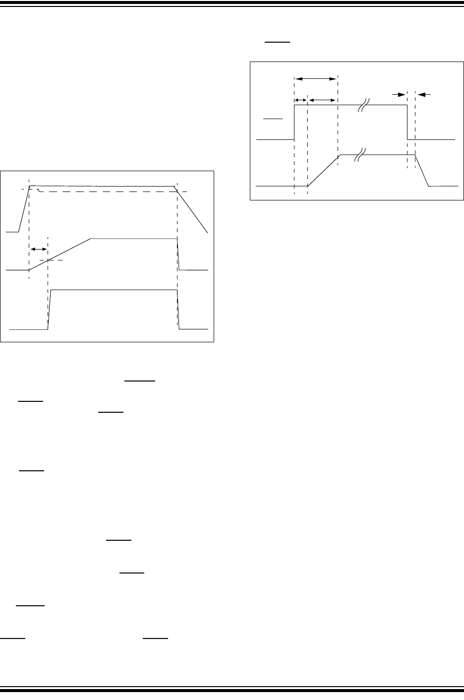
4.7 Shutdown Input (SHDN)
The SHDN input is an active-low input signal that turns
the LDO on and off. The SHDN threshold is a percent-
age of the input voltage. The typical value of this
shutdown threshold is 30% of V
IN
, with minimum and
maximum limits over the entire operating temperature
range of 45% and 15%, respectively.
The SHDN
input will ignore low-going pulses (pulses
meant to shut down the LDO) that are up to 400 ns in
pulse width. If the shutdown input is pulled low for more
than 400 ns, the LDO will enter Shutdown mode. This
small bit of filtering helps to reject any system noise
spikes on the shutdown input signal.
On the rising edge of the SHDN
input, the shutdown
circuitry has a 30 µs delay before allowing the LDO
output to turn on. This delay helps to reject any false
turn-on signals or noise on the SHDN
input signal. After
the 30 µs delay, the LDO output enters its soft-start
period as it rises from 0V to its final regulation value. If
the SHDN
input signal is pulled low during the 30 µs
delay period, the timer will be reset and the delay time
will start over again on the next rising edge of the
SHDN
input. The total time from the SHDN input going
high (turn-on) to the LDO output being in regulation is
typically 100 µs. See Figure 4-5 for a timing diagram of
the SHDN
input.
FIGURE 4-5: Shutdown Input Timing
Diagram.
4.8 Dropout Voltage and Undervoltage
Lockout
Dropout voltage is defined as the input-to-output
voltage differential at which the output voltage drops
2% below the nominal value that was measured with a
V
R
+ 0.5V differential applied. The MCP1726 LDO has
a very low dropout voltage specification of 220 mV
(typical) at 1A of output current. See the Electrical
Characteristics table for maximum dropout voltage
specifications.
The MCP1726 LDO operates across an input voltage
range of 2.3V to 6.0V and incorporates input Undervolt-
age Lockout (UVLO) circuitry that keeps the LDO
output voltage off until the input voltage reaches a
minimum of 2.18V (typical) on the rising edge of the
input voltage. As the input voltage falls, the LDO output
will remain on until the input voltage level reaches
2.04V (typical).
Since the MCP1726 LDO undervoltage lockout
activates at 2.04V as the input voltage is falling, the
dropout voltage specification does not apply for output
voltages that are less than 1.9V.
For high-current applications, voltage drops across the
PCB traces must be taken into account. The trace
resistances can cause significant voltage drops
between the input voltage source and the LDO. For
applications with input voltages near 2.3V, these PCB
trace voltage drops can sometimes lower the input
voltage enough to trigger a shutdown due to
undervoltage lockout.
V
OUT
T
PG
V
PWRGD_TH
C
DELAY
C
DELAY
Threshold (0.42V)
PWRGD
0V
1.5V (typ)
SHDN
V
OUT
30 µs
70 µs
T
OR
400 ns (typ)