
Datasheet

2012-2013 Microchip Technology Inc. DS20005122B-page 11
MCP1703A
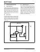
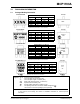
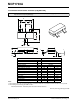
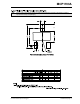
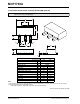
3.0 PIN DESCRIPTIONS
The descriptions of the pins are listed in Table 3-1.
3.1 Ground Terminal (GND)
Regulator ground. Tie GND to the negative side of the
output and the negative side of the input capacitor.
There is no high current and only the LDO bias current
(2.0 µA typical) flows out of this pin. The LDO output
regulation is referenced to this pin. Minimize voltage
drops between this pin and the negative side of the
load.
3.2 Regulated Output Voltage (V
OUT
)
Connect V
OUT
to the positive side of the load and the
positive terminal of the output capacitor. The positive
side of the output capacitor should be physically
located close to the LDO V
OUT
pin as is practical. The
current flowing out of this pin is equal to the DC load
current.
3.3 Unregulated Input Voltage (V
IN
)
Connect V
IN
to the input unregulated source voltage.
Like all low dropout linear regulators, low source
impedance is necessary for stable operation of the
LDO. The amount of capacitance required to ensure
low source impedance depends on the proximity of the
input source capacitors or battery type. For most
applications, 1 µF of capacitance ensures stable
operation of the LDO circuit. The input capacitance
requirement can be lowered for applications that have
load currents below 100 mA. The type of capacitor
used can be ceramic, tantalum or aluminum
electrolytic. The low ESR characteristics of the ceramic
yields better noise and PSRR performance at
high-frequency.
3.4 Exposed Thermal Pad (EP)
An internal electrical connection between the Exposed
Thermal Pad (EP) and the V
SS
pin. They must be
connected to the same potential on the Printed Circuit
Board (PCB).
TABLE 3-1: MCP1703A PIN FUNCTION TABLE
2x3 DFN SOT-223 SOT-23A SOT-89 Name Function
4 2,Tab 1 1 GND Ground Terminal
1 323V
OUT
Regulated Voltage Output
8132,TabV
IN
Unregulated Supply Voltage
2, 3, 5, 6, 7 — — — NC No Connection
9 — — — EP Exposed Thermal Pad (EP); must be
connected to VSS