
Datasheet

MCP1703A
DS20005122B-page 14 2012-2013 Microchip Technology Inc.
6.0 APPLICATION CIRCUITS AND
ISSUES
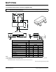
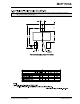
6.1 Typical Application
The MCP1703A is most commonly used as a voltage
regulator. Its low quiescent current and low dropout
voltage make it ideal for many battery-powered
applications.
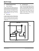
FIGURE 6-1: Typical Application Circuit.
6.1.1 APPLICATION INPUT CONDITIONS
6.2 Power Calculations
6.2.1 POWER DISSIPATION
The internal power dissipation of the MCP1703A is a
function of input voltage, output voltage and output
current. As a result of the quiescent current draw, the
power dissipation is so low that it is insignificant (2.0 µA
x V
IN
). The following equation can be used to calculate
the internal power dissipation of the LDO.
EQUATION 6-1:
The maximum continuous operating junction
temperature specified for the MCP1703A is +125°C
. To
estimate the internal junction temperature of the
MCP1703A, the total internal power dissipation is
multiplied by the thermal resistance from junction to
ambient (Rθ
JA
). The thermal resistance from junction
to ambient for the SOT-23A pin package is estimated at
336°C/W.
EQUATION 6-2:
The maximum power dissipation capability for a
package can be calculated given the junction-to-
ambient thermal resistance and the maximum ambient
temperature for the application. The following equation
can be used to determine the package maximum
internal power dissipation.
EQUATION 6-3:
EQUATION 6-4:
EQUATION 6-5:
Package Type = SOT-23A
Input Voltage Range = 2.7V to 4.8V
V
IN
maximum = 4.8V
V
OUT
typical = 1.8V
I
OUT
= 50 mA maximum
GND
V
OUT
V
IN
C
IN
1 µF Ceramic
C
OUT
1µF Ceramic
V
OUT
V
IN
2.7V to 4.8V
1.8V
I
OUT
50 mA
MCP1703A
P
LDO
V
IN MAX()
V
OUT MIN()
–()I
OUT MAX()
×=
Where:
P
LDO
= LDO Pass device internal power
dissipation
V
IN(MAX)
= Maximum input voltage
V
OUT(MIN)
= LDO minimum output voltage
T
JMAX()
P
TOTAL
Rθ
JA
× T
AMAX()
+=
Where:
T
J(MAX)
= Maximum continuous junction
temperature
P
TOTAL
= Total device power dissipation
Rθ
JA
= Thermal resistance from
junction-to-ambient
T
A(MAX)
= Maximum ambient temperature
P
DMAX()
T
JMAX()
T
AMAX()
–()
Rθ
JA
---------------------------------------------------
=
Where:
P
D(MAX)
= Maximum device power dissipation
T
J(MAX)
= Maximum continuous junction
temperature
T
A(MAX)
= Maximum ambient temperature
Rθ
JA
= Thermal resistance from
junction-to-ambient
T
JRISE()
P
DMAX()
Rθ
JA
×=
Where:
T
J(RISE)
= Rise in device junction temperature
over the ambient temperature
P
TOTAL
= Maximum device power dissipation
Rθ
JA
= Thermal resistance from junction to
ambient
T
J
T
JRISE()
T
A
+=
Where:
T
J
= Junction temperature
T
J(RISE)
= Rise in device junction temperature
over the ambient temperature
T
A
= Ambient temperature