
Datasheet

MCP1703A
DS20005122B-page 12 2012-2013 Microchip Technology Inc.
4.0 DETAILED DESCRIPTION
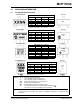
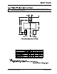
4.1 Output Regulation
A portion of the LDO output voltage is fed back to the
internal error amplifier and compared with the precision
internal band gap reference. The error amplifier output
adjusts the amount of current that flows through the P-
Channel pass transistor, thus regulating the output
voltage to the desired value. Any changes in input
voltage or output current causes the error amplifier to
respond and adjust the output voltage to the target
voltage (see Figure 4-1).
4.2 Overcurrent
The MCP1703A internal circuitry monitors the amount
of current flowing through the P-Channel pass
transistor. In the event of a short-circuit or excessive
output current, the MCP1703A turns off the P-Channel
device for a short period, after which the LDO attempts
to restart. If the excessive current remains, the cycle
will repeat itself.
4.3 Overtemperature
The internal power dissipation within the LDO is a
function of input-to-output voltage differential and load
current. If the power dissipation within the LDO is
excessive, the internal junction temperature rises
above the typical shutdown threshold of 150°C. At that
point, the LDO shuts down and begins to cool to the
typical turn-on junction temperature of 130°C. If the
power dissipation is low enough, the device will
continue to cool and operate normally. If the power
dissipation remains high, the thermal shutdown
protection circuitry will again turn off the LDO,
protecting it from catastrophic failure.
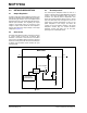
FIGURE 4-1: Block Diagram.
+
-
V
IN
V
OUT
GND
+V
IN
Error Amplifier
Voltage
Reference
Overcurrent
Overtemperature
MCP1703A