
User`s guide


MCP1630 BOOST MODE LED DRIVER
DEMO BOARD USER’S GUIDE
© 2007 Microchip Technology Inc. DS51665B-page 21
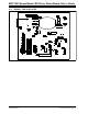
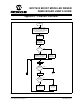
Appendix C. Firmware Flowchart
FIGURE C-1: Firmware Flowchart - Page 1.
Start
Output V
REF
Signal
through GP5
(Reference Voltage for
MCP1630 )
Setup CCP module
and 20% duty cycle
(Clock for MCP1630)
Is GP1 = 1?
YES
NO
Clear the
Potentiometer flag
Start ADC
ADC
or Channel3
CH1
CH3
Set ADC for CH3
Is
Potentiometer
Flag set?
YES
Set DimDuty for the
potentiometer output
value
NO
Set DimDuty
for maximum
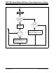
A
B
Initialize: GP2 (for Output PWM)
And GP5 (for Output V
REF
Internal Osc Clock to 8 MHz, TMR0 = 0
Configure Ansel & CMCON0 as Digital I/O
Set Weak Pull-Up on GP1
1. Clear Weak Pull-Up on GP1
2. Set a Flag for Potentiometer
Detected
3. Set GP1 for Analog Input
Channel1
duty cycle