
User`s guide


MCP1630 Boost Mode LED Driver Demo Board User’s Guide
DS51665B-page 10 © 2007 Microchip Technology Inc.
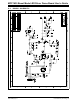
The CCP output is also connected to a simple ramp generator that is reset at the begin-
ning of each MCP1630 clock cycle. The ramp generator is composed of transistor Q2,
resistors R2, R3 and capacitor C6. It provides the reference signal to the MCP1630
comparator. The MCP1630 comparator compares this ramp reference signal to the
error amplifier output to generate a PWM signal.
A resistor voltage divider (R4, R5 and R6) and filter is used to set the reference voltage
for the constant current control and is driven by the GP5 pin of the MCU. Jumper J4 is
used to select two different reference voltages to drive the LED load at different current
levels. With J4 removed, resistors R4 and R5 provide a 206 mV reference voltage. This
setting provides 350 mA output current. With J4 installed, resistors R4, R5 and R6
provide a 412 mV reference voltage. (700 mA output)
R8 and C7 form an integrator circuit in the negative feedback path, providing high loop
gain at DC. This simple compensation network is sufficient for a constant current LED
driver. Places have been provided on the PCB for additional compensation
components, if required.
R12 and R13 form a voltage divider that is used to monitor the output voltage of the
boost circuit. The output of the voltage divider is connected to pin GP4 of the MCU and
monitored with the ADC.
L1, Q1, D2, C12, and C13 form the basic voltage boost circuit. C13 is not populated on
the PCB. The value of C12 has been selected to keep the LED current ripple less than
20% at the rated load conditions.
2.5 FIRMWARE DESCRIPTION
Appendix C shows the firmware flowchart. Different parts of the firmware operation are
described below.
2.5.1 Clock Generation
At a minimum, the PIC12F683 code must initialize the CCP module in PWM mode to
produce a clock signal for the MCP1630. The CCP is configured to produce 500 kHz
with a 20% duty cycle. The clock duty cycle limits the maximum on time of the power
MOSFET to 80% duty. I/O pins GP5 is driven high to enable the voltage reference for
the MCP1630 control loop. After these tasks are completed, the MCP1630 can begin
the current regulation function and the MCU can execute other tasks.
2.5.2 Open Circuit Detection
One potential problem that can occur with a constant current application is an open-cir-
cuit load condition. In this case, the power supply will try to raise the output voltage to
provide the required current. A boost converter circuit can continue to raise the output
voltage until component damage occurs. The software monitors the output voltage to
the MCP1630 using an ADC channel and disables the power supply when a maximum
output voltage of 40V is reached.
Once the output reference voltage reaches the allowable maximum limit, the GP2 pin
is driven high by writing a 100% duty cycle value to the CCP control registers. This high
signal effectively resets the MCP1630. The reference to the MCP1630 is also disabled
by clearing pin GP5. After the over-voltage event, the software provides a delay before
restarting the input clock to the MCP1630 PWM generator and turning on the reference
voltage. The delay reduces stress on the power supply components.