
User`s guide


Installation and Operation
© 2007 Microchip Technology Inc. DS51665B-page 9
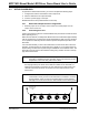
2.3.3 Powering the MCP1630 Boost Mode LED Driver Demo Board
1. Connect a power supply to J1 to power up the MCP1630 Boost Mode LED Driver
Demo Board. Ensure that the power supply has a 2.5 mm barrel connector with
the center pin positive. The input voltage source should be limited to the 9V to
+16V range. Ensure that the chosen power supply can provide enough current
at the selected voltage to properly power the LEDs.
An external potentiometer can be connected to the MCU to provide LED dimming
control. The 'Dimming Control' section of this document provides more information.
2.3.4 Verifying the Application
The best way to evaluate the MCP1630 is to dig into the circuit and measure voltages
and currents with a multi-meter and probe the board with an oscilloscope. You can use
the following procedure to verify the LED input power:
1. To measure the output voltage (V
LED
), connect the multi-meter across TP1 and
TP2.
2. The load current (I
LED
) passes through the LED load as well as current sense
resistor, R14. To measure the output current, connect the multi-meter across TP2
and TP3 to determine the voltage drop across R14. The current through resistor
R14 and the load is VR14 / R14.
3. The output power can be calculated as P
LED
= I
LED
* V
LED
.
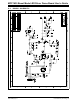
2.4 CIRCUIT DESCRIPTION
Appendix A shows the circuit schematic for the MCP1630 Boost Mode LED Driver
Demo Board.
The input voltage to the circuit may vary from +9 V to +16 V. The MCP1702 voltage
regulator U1 generates a regulated 5 V output for the MCP1630 and the PIC12F683
devices. A 12V Zener diode, D1, is used to limit the maximum input voltage to the
MCP1702 device.
The MCP1630 PWM controller (U3) is comprised of a high-speed comparator, high
bandwidth amplifier and set/reset flip flop, and high current driver pin. It has the
necessary components to develop an analog switch-mode power supply control loop.
The MCP1630 is designed to operate from an external clock source. The clock
frequency sets the power supply switching frequency and the clock duty cycle sets the
maximum duty cycle for the supply.
The PIC12F683 MCU (U2) operates from its own 8 MHz internal oscillator and has an
on chip Capture/Compare/PWM (CCP) peripheral module. When operating in PWM
mode, the CCP module can generate a pulse-width modulated signal with variable fre-
quency and duty cycles.
The CCP output of the MCU is connected to the oscillator input of the MCP1630 device.
For this application, the CCP module is configured to provide a 500 kHz clock source
with 20% duty cycle. The 20% duty cycle produced by the CCP module limits the
maximum duty cycle of the MCP1630 to 80%. Once configured, the CCP peripheral
does not need any control by the MCU software. If desired, the CCP can be reconfig-
ured to obtain different clock frequencies up to the 2 MHz maximum specification for
the MCP1630.
Note: The LEDs will be very bright during operation and provide a focused light
source! Avoid looking directly into the LEDs when power is applied to the
circuit. It is recommended that you cover the string of LEDs with a sheet of
paper or some other opaque material during testing to avoid discomfort.