
Datasheet


© 2008 Microchip Technology Inc. DS22062B-page 3
MCP14E3/MCP14E4/MCP14E5
1.0 ELECTRICAL
CHARACTERISTICS
Absolute Maximum Ratings †
Supply Voltage................................................................+20V
Input Voltage ...............................(V
DD
+ 0.3V) to (GND – 5V)
Enable Voltage.............................(V
DD
+ 0.3V) to (GND - 5V)
Input Current (V
IN
>V
DD
)................................................50 mA
Package Power Dissipation (T
A
= 50°C)
8L-DFN ....................................................................... Note 3
8L-PDIP ........................................................................1.10W
8L-SOIC .....................................................................665 mW
† Notice: Stresses above those listed under "Maximum
Ratings" may cause permanent damage to the device. This is
a stress rating only and functional operation of the device at
those or any other conditions above those indicated in the
operational sections of this specification is not intended.
Exposure to maximum rating conditions for extended periods
may affect device reliability.
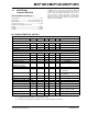
DC CHARACTERISTICS (NOTE 2)
Electrical Specifications: Unless otherwise indicated, T
A
= +25°C, with 4.5V ≤ V
DD
≤ 18V.
Parameters Sym Min Typ Max Units Conditions
Input
Logic ‘1’, High Input Voltage V
IH
2.4 1.5 — V
Logic ‘0’, Low Input Voltage V
IL
—1.30.8V
Input Current I
IN
–1 — 1 µA 0V ≤ V
IN
≤ V
DD
Input Voltage V
IN
-5 — V
DD
+0.3 V
Output
High Output Voltage V
OH
V
DD
– 0.025 — — V DC Test
Low Output Voltage V
OL
— — 0.025 V DC Test
Output Resistance, High R
OH
—2.53.5Ω I
OUT
= 10 mA, V
DD
= 18V
Output Resistance, Low R
OL
—2.53.0Ω I
OUT
= 10 mA, V
DD
= 18V
Peak Output Current I
PK
—4.0—AV
DD
= 18V (Note 2)
Latch-Up Protection With-
stand Reverse Current
I
REV
— >1.5 — A Duty cycle ≤ 2%, t ≤ 300 µs
Switching Time (Note 1)
Rise Time t
R
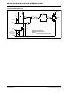
—1530nsFigure 4-1, Figure 4-2
C
L
= 2200 pF
Fall Time t
F
—1830nsFigure 4-1, Figure 4-2
C
L
= 2200 pF
Propagation Delay Time t
D1
—4655nsFigure 4-1, Figure 4-2
Propagation Delay Time t
D2
—5055nsFigure 4-1, Figure 4-2
Enable Function (ENB_A, ENB_B)
High-Level Input Voltage V
EN_H
1.60 1.90 2.90 V V
DD
= 12V, LO to HI Transition
Low-Level Input Voltage V
EN_L
1.30 2.20 2.40 V V
DD
= 12V, HI to LO Transition
Hysteresis V
HYST
0.10 0.30 0.60 V
Enable Leakage Current I
ENBL
40 85 115 µA V
DD
=12V,
ENB_A = ENB_B = GND
Propagation Delay Time t
D3
—60—nsFigure 4-3 (Note 1)
Propagation Delay Time t
D4
—50—nsFigure 4-3 (Note 1)
Note 1: Switching times ensured by design.
2: Tested during characterization, not production tested.
3: Package power dissipation is dependent on the copper pad area on the PCB.