
Datasheet


© 2007 Microchip Technology Inc. DS22052B-page 9
MCP1401/02
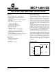
3.0 PIN DESCRIPTIONS
The descriptions of the pins are listed in Table 3-1.
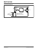
TABLE 3-1: PIN FUNCTION TABLE
(1)
3.1 Supply Input (V
DD
)
V
DD
is the bias supply input for the MOSFET driver and
has a voltage range of 4.5V to 18V. This input must be
decoupled to ground with a local capacitor. This bypass
capacitor provides a localized low-impedance path for
the peak currents that are to be provided to the load.
3.2 Control Input (IN)
The MOSFET driver input is a high-impedance, TTL/
CMOS-compatible input. The input also has hysteresis
between the high and low input levels, allowing them to
be driven from slow rising and falling signals, and to
provide noise immunity.
3.3 Ground (GND)
Ground is the device return pin. The ground pin should
have a low impedance connection to the bias supply
source return. High peak currents will flow out the
ground pin when the capacitive load is being
discharged.
3.4 Output (OUT)
The output is a CMOS push-pull output that is capable
of sourcing and sinking 0.5A of peak current
(V
DD
= 18V). The low output impedance ensures the
gate of the external MOSFET will stay in the intended
state even during large transients. This output also has
a reverse current latch-up rating of 0.5A.
SOT-23-5 Symbol Description
1 GND Ground
2V
DD
Supply Input
3 IN Control Input
4 GND Ground
5 OUT Output
Note 1: Duplicate pins must be connected for proper operation.