
Datasheet
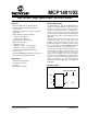


MCP1401/02
DS22052B-page 4 © 2007 Microchip Technology Inc.
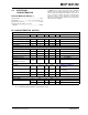
DC CHARACTERISTICS (OVER OPERATING TEMPERATURE RANGE)
TEMPERATURE CHARACTERISTICS
Electrical Specifications: Unless otherwise indicated, operating temperature range with 4.5V ≤ V
DD
≤ 18V.
Parameters Sym Min Typ Max Units Conditions
Input
Logic ‘1’, High Input Voltage V
IH
2.4 — — V
Logic ‘0’, Low Input Voltage V
IL
——0.8V
Input Current I
IN
–10 — +10 µA 0V ≤ V
IN
≤ V
DD
Input Voltage V
IN
-5 — V
DD
+0.3 V
Output
High Output Voltage V
OH
V
DD
– 0.025 — — V DC TEST
Low Output Voltage V
OL
— — 0.025 V DC TEST
Output Resistance, High R
OH
—1218Ω I
OUT
= 10 mA, V
DD
= 18V
Output Resistance, Low R
OL
—1016Ω I
OUT
= 10 mA, V
DD
= 18V
Switching Time (Note 1)
Rise Time t
R
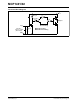
—2030nsFigure 4-1, Figure 4-2
C
L
= 470 pF
Fall Time t
F
—1828nsFigure 4-1, Figure 4-2
C
L
= 470 pF
Delay Time t
D1
—4051nsFigure 4-1, Figure 4-2
Delay Time t
D2
—4051nsFigure 4-1, Figure 4-2
Power Supply
Supply Voltage V
DD
4.5 — 18.0 V
Power Supply Current I
S
—
—
0.90
0.11
1.10
0.20
mA
mA
V
IN
= 3V
V
IN
= 0V
Note 1: Switching times ensured by design.
2: Tested during characterization, not production tested.
Electrical Specifications: Unless otherwise noted, all parameters apply with 4.5V ≤ V
DD
≤ 18V.
Parameters Sym Min Typ Max Units Conditions
Temperature Ranges
Specified Temperature Range T
A
–40 — +125 °C
Maximum Junction Temperature T
J
— — +150 °C
Storage Temperature Range T
A
–65 — +150 °C
Package Thermal Resistances
Thermal Resistance, 5L-SOT-23 θ
JA
—256 —°C/W