
Datasheet


MCP1401/02
DS22052B-page 10 © 2007 Microchip Technology Inc.
4.0 APPLICATION INFORMATION
4.1 General Information
MOSFET drivers are high-speed, high current devices
which are intended to source/sink high peak currents to
charge/discharge the gate capacitance of external
MOSFETs or IGBTs. In high frequency switching power
supplies, the PWM controller may not have the drive
capability to directly drive the power MOSFET. A
MOSFET driver like the MCP1401/02 family can be
used to provide additional source/sink current
capability.
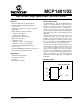
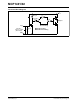
4.2 MOSFET Driver Timing
The ability of a MOSFET driver to transition from a fully
off state to a fully on state are characterized by the
drivers rise time (t
R
), fall time (t
F
), and propagation
delays (t
D1
and t
D2
). The MCP1401/02 family of drivers
can typically charge and discharge a 470 pF load
capacitance in 19 ns along with a typical matched
propagation delay of 35 ns. Figure 4-1 and Figure 4-2
show the test circuit and timing waveform used to verify
the MCP1401/02 timing.
FIGURE 4-1: Inverting Driver Timing
Waveform.
FIGURE 4-2: Non-Inverting Driver Timing
Waveform.
4.3 Decoupling Capacitors
Careful layout and decoupling capacitors are highly
recommended when using MOSFET drivers. Large
currents are required to charge and discharge
capacitive loads quickly. For example, approximately
550 mA are needed to charge a 470 pF load with 18V
in 15 ns.
To operate the MOSFET driver over a wide frequency
range with low supply impedance, a ceramic and low
ESR film capacitor is recommended to be placed in
parallel between the driver V
DD
and GND. A 1.0 µF low
ESR film capacitor and a 0.1 µF ceramic capacitor
placed between pins 2 and 1 should be used. These
capacitors should be placed close to the driver to
minimized circuit board parasitics and provide a local
source for the required current.
4.4 PCB Layout Considerations
Proper PCB layout is important in a high current, fast
switching circuit to provide proper device operation and
robustness of design. PCB trace loop area and
inductance should be minimized by the use of ground
planes or trace under MOSFET gate drive signals,
separate analog and power grounds, and local driver
decoupling.
Placing a ground plane beneath the MCP1401/02 will
help as a radiated noise shield as well as providing
some heat sinking for power dissipated within the
device.
0.1 µF
+5V
10%
90%
10%
90%
10%
90%
18V
1µF
0V
0V
MCP1401
C
L
= 470 pF
Input
Input
Output
t
D1
t
F
t
D2
Output
t
R
V
DD
= 18V
Ceramic
90%
Input
t
D1
t
F
t
D2
Output
t
R
10%
10%
10%
+5V
18V
0V
0V
90%
90%
0.1 µF
1µF
MCP1402
C
L
= 470 pF
Input Output
V
DD
= 18V
Ceramic