
Datasheet


Table Of Contents
- Device Features
- 1.0 Electrical Characteristics
- 2.0 Typical Performance Curves
- 3.0 PIN Description
- 4.0 Operational Description
- 5.0 Application Information
- 5.1 Supply Monitor Noise Sensitivity
- 5.2 Conventional Voltage Monitoring
- 5.3 Using in PIC® Microcontroller, ICSP™ Applications
- 5.4 Modifying The Trip Point, VTRIP
- 5.5 MOSFET Low-Drive Protection
- 5.6 Low-Power Applications
- 5.7 Controllers and Processors With Bidirectional I/O Pins
- 5.8 RESET Signal Integrity During Power-Down
- 6.0 Standard Device Offerings
- 7.0 Development Tools
- 8.0 Packaging Information
- Appendix A: Revision History
- Product Identification System
- Trademarks
- Worldwide Sales and Service
2005-2012 Microchip Technology Inc. DS21985D-page 3
MCP131X/2X
1.0 ELECTRICAL
CHARACTERISTICS
Absolute Maximum Ratings†
Supply Voltage (V
DD
to V
SS
). . . . . . . . . . . . . . . . . . . . . . 7.0V
Input current (V
DD
) . . . . . . . . . . . . . . . . . . . . . . . . . . . .10 mA
Output current (RST
) . . . . . . . . . . . . . . . . . . . . . . . . . .10 mA
Voltage on all inputs and outputs, except Open-Drain RS
T
(with no internal pull-up resistor), w.r.t. V
SS
. .-0.6V to (V
DD
+
1.0V)
Voltage on Open-Drain RST
(with no internal pull-up resistor) w.r.t. V
SS
. . -0.6V to 13.5V
Storage temperature . . . . . . . . . . . . . . . . . . .-65°C to +150°C
Ambient temp. with power applied . . . . . . . .-40°C to +125°C
Maximum Junction temp. with power applied . . . . . . .+150°C
Power Dissipation (T
A
+70°C):
5-Pin SOT-23A .......................................................240 mW
ESD protection on all pins 4kV
† Notice: Stresses above those listed under “Maximum Rat-
ings” may cause permanent damage to the device. This is a
stress rating only and functional operation of the device at
those or any other conditions above those indicated in the
operational listings of this specification is not implied. Expo-
sure to maximum rating conditions for extended periods may
affect device reliability.
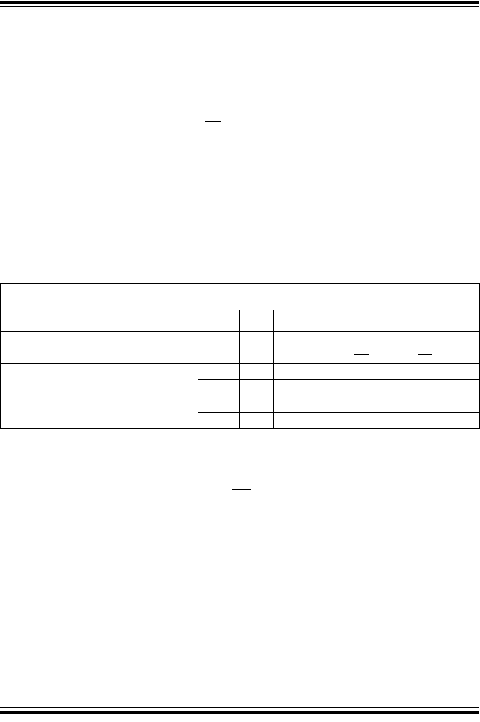
DC CHARACTERISTICS
Electrical Specifications: Unless otherwise indicated, all limits are specified for V
DD
= 1V to 5.5V, R
PU
= 100 k
(only MCP1320, MCP1321 and MCP1322), T
A
= -40°C to +125°C.
Parameters Sym Min Typ Max Units Conditions
Operating Voltage Range V
DD
1.0 — 5.5 V
Specified V
DD
Value to V
OUT
Low V
DD
1.0 — — V I
RST
= 10 µA, V
RST
< 0.3V
Operating Current: I
DD
— 5 10 µA Watchdog Timer Active
— 1 2 µA Watchdog Timer Inactive
—12µAV
DD
< V
TRIP
— 5 10 µA Reset Delay Timer Active
Note 1: Trip point is ±1.5% from typical value.
2: Trip point is ±2.5% from typical value.
3: Hysteresis is minimum = 1%, maximum = 6% at +25°C.
4: This specification allows this device to be used in PIC
®
microcontroller applications that require the In-
Circuit Serial Programming™ (ICSP™) feature (see device-specific programming specifications for
voltage requirements). The total time that the RST
pin can be above the maximum device operational
voltage (5.5V) is 100s. Current into the RST
pin should be limited to 2 mA. It is recommended that the
device operational temperature be maintained between 0°C to +70°C (+25°C preferred). For additional
information, refer to Figure 2-35.
5: This parameter is established by characterization and is not 100% tested.
6: Custom ordered voltage trip point; minimum order volume requirement. Information available upon request.