
User manual


MCP1256/7/8/9 Charge Pump Evaluation Board User’s Guide
DS51603A-page 8 © 2006 Microchip Technology Inc.
2.3 GETTING STARTED
The MCP1256/7/8/9 Evaluation Board is fully assembled and tested for generating a
regulated 3.3V output voltage from a 1.8V to 3.6V input at load currents up to 100 mA.
The board requires the use of an external input voltage source and external load.
2.3.1 Power Input and Output Connections
2.3.1.1 POWERING THE MCP1256/7/8/9 EVALUATION BOARD
1. Apply the input voltage source to the appropriate circuit for evaluation. The input
voltage source should be limited to the 0V to +3.6V range. For normal operation,
the input voltage should be between +1.8V and +3.6V. The input voltage must
not exceed an absolute maximum of +3.8V.
2. Connect the positive side of the input source (+) to V
IN
of the circuit being
evaluated. Connect the negative or return side of the input source (-) to GND of
the circuit being evaluated. Refer to Figure 2-1.
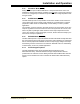
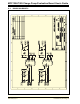
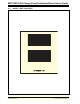
FIGURE 2-1: Setup Configuration Diagram.
2.3.1.2 APPLYING THE LOAD TO THE MCP1256/7/8/9 EVALUATION BOARD
1. To apply a load to a MCP1256/7/8/9 Evaluation Board, the positive side of the
load (+) should be connected to V
OUT
of the circuit being evaluated.
2. The negative or return side of the load (-) should be connected to GND of the
circuit being evaluated. Care should be taken when using electronic loads or
ground referenced loads.
C5
R4
C1
R1
C6
R6
C2
R3
U2
TP 9 TP 10
TP 5
U1
TP 2 TP 3
C7 C8
R5
TP 12
TP 14
C3 C4
R2
TP 7
TP 8
TP 4
TP 1
TP 11
TP 13
TP 6
Input
Power Supply
1.8V to 3.6V
+
_
Input
Power Supply
1.8V to 3.6V
+
_
+
_
+
_
Output
Load
Output
Load