MCP1256/7/8/9 Charge Pump Evaluation Board User’s Guide © 2006 Microchip Technology Inc.
Note the following details of the code protection feature on Microchip devices: • Microchip products meet the specification contained in their particular Microchip Data Sheet. • Microchip believes that its family of products is one of the most secure families of its kind on the market today, when used in the intended manner and under normal conditions. • There are dishonest and possibly illegal methods used to breach the code protection feature.
MCP1256/7/8/9 CHARGE PUMP EVALUATION BOARD USER’S GUIDE Table of Contents Preface ........................................................................................................................... 1 Chapter 1. Product Overview ....................................................................................... 5 1.1 Introduction ..................................................................................................... 5 1.2 What is the MCP1256/7/8/9 Charge Pump Evaluation Board? .....
MCP1256/7/8/9 Charge Pump Evaluation Board User’s Guide NOTES: DS51603A-page iv © 2006 Microchip Technology Inc.
MCP1256/7/8/9 CHARGE PUMP EVALUATION BOARD USER’S GUIDE Preface NOTICE TO CUSTOMERS All documentation becomes dated, and this manual is no exception. Microchip tools and documentation are constantly evolving to meet customer needs, so some actual dialogs and/or tool descriptions may differ from those in this document. Please refer to our web site (www.microchip.com) to obtain the latest documentation available. Documents are identified with a “DS” number.
MCP1256/7/8/9 Charge Pump Evaluation Board User’s Guide CONVENTIONS USED IN THIS GUIDE This manual uses the following documentation conventions: DOCUMENTATION CONVENTIONS Description Arial font: Italic characters Initial caps Quotes Underlined, italic text with right angle bracket Bold characters N‘Rnnnn Text in angle brackets < > Courier New font: Plain Courier New Represents Examples Referenced books Emphasized text A window A dialog A menu selection A field name in a window or dialog A menu path MP
Preface THE MICROCHIP WEB SITE Microchip provides online support via our web site at www.microchip.com. This web site is used as a means to make files and information easily available to customers.
MCP1256/7/8/9 Charge Pump Evaluation Board User’s Guide NOTES: DS51603A-page 4 © 2006 Microchip Technology Inc.
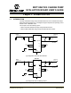
MCP1256/7/8/9 CHARGE PUMP EVALUATION BOARD USER’S GUIDE Chapter 1. Product Overview 1.1 INTRODUCTION The MCP1256/7/8/9 Charge Pump Evaluation Board is used to evaluate Microchip’s MCP1256/7/8/9 Regulated 3.3V, Low-Ripple Charge Pumps with low-operating current SLEEP mode or BYPASS mode. This chapter covers the following topics: • What is the MCP1256/7/8/9 Charge Pump Evaluation Board? • What the MCP1256/7/8/9 Charge Pump Evaluation Board Includes MCP1256 INPUT 1.6V to 3.6V 7 CIN VIN VOUT OUTPUT 3.
MCP1256/7/8/9 Charge Pump Evaluation Board User’s Guide 1.2 WHAT IS THE MCP1256/7/8/9 CHARGE PUMP EVALUATION BOARD? The MCP1256/7/8/9 Charge Pump Evaluation Board is an evaluation and demonstration tool for Microchip Technology’s MCP1256/7/8/9 Regulated 3.3V, Low-Ripple Charge Pumps with low-operating current SLEEP mode or BYPASS mode. The design provides for dynamic versatility. The MCP1256/7/8/9 Charge Pump Evaluation Board is setup to evaluate simple, stand-alone, DC-to-DC conversion.
MCP1256/7/8/9 CHARGE PUMP EVALUATION BOARD USER’S GUIDE Chapter 2. Installation and Operation 2.1 INTRODUCTION The MCP1256/7/8/9 Charge Pump Evaluation Board demonstrates Microchip’s MCP1256/7/8/9 devices. The MCP1256/7/8/9 devices are positive regulated charge pumps that accept an input voltage from +1.8V to +3.6V and convert it to a regulated 3.3V output voltage.
MCP1256/7/8/9 Charge Pump Evaluation Board User’s Guide 2.3 GETTING STARTED The MCP1256/7/8/9 Evaluation Board is fully assembled and tested for generating a regulated 3.3V output voltage from a 1.8V to 3.6V input at load currents up to 100 mA. The board requires the use of an external input voltage source and external load. 2.3.1 Power Input and Output Connections 2.3.1.1 POWERING THE MCP1256/7/8/9 EVALUATION BOARD 1. Apply the input voltage source to the appropriate circuit for evaluation.
Installation and Operation 2.3.2 Shutdown Mode (SHDN) Driving SHDN low puts the MCP1256/7/8/9 in a low-power Shutdown mode. This disables the charge-pump switches, oscillator and control logic, reducing the quiescent current to 0.1 μA (typical). The PGOOD output and LBO are in a high impedance state during shutdown. 2.3.3 SLEEP Mode (SLEEP) The MCP1256/7 provide a unique SLEEP mode feature.
MCP1256/7/8/9 Charge Pump Evaluation Board User’s Guide NOTES: DS51603A-page 10 © 2006 Microchip Technology Inc.
MCP1256/7/8/9 CHARGE PUMP EVALUATION BOARD USER’S GUIDE Appendix A. Schematic and Layouts A.1 INTRODUCTION This appendix contains the following schematic and layouts for the MCP1256/7/8/9 Charge Pump Evaluation Board. Diagrams included in this appendix: • • • • • Board Schematic Board - Assembly Drawing Board - Top Overlay Board - Top Layer Board - Bottom Layer © 2006 Microchip Technology Inc.
MCP1256/7/8/9 Charge Pump Evaluation Board User’s Guide A.2 BOARD SCHEMATIC DS51603A-page 12 © 2006 Microchip Technology Inc.
Schematic and Layouts © 2006 Microchip Technology Inc. TP 14 TP 12 C6 TP 13 TP 8 TP 11 C5 R4 C7 R5 C8 TP 10 TP 9 R6 U2 TP 7 TP 5 C2 C4 C1 TP 6 TP 4 TP 1 R1 C3 R2 TP 2 R3 TP 3 BOARD - ASSEMBLY DRAWING U1 A.
MCP1256/7/8/9 Charge Pump Evaluation Board User’s Guide A.4 BOARD - TOP OVERLAY TP 1 R1 TP 2 R3 R2 U1 TP 4 TP 5 TP 6 TP 7 C1 C3 C4 TP 8 R4 C2 TP 9 R6 R5 U2 TP 11 TP 10 TP 12 TP 13 TP 14 C5 DS51603A-page 14 TP 3 C7 C8 C6 © 2006 Microchip Technology Inc.
Schematic and Layouts A.5 BOARD - TOP LAYER © 2006 Microchip Technology Inc.
MCP1256/7/8/9 Charge Pump Evaluation Board User’s Guide A.6 BOARD - BOTTOM LAYER DS51603A-page 16 © 2006 Microchip Technology Inc.
MCP1256/7/8/9 CHARGE PUMP EVALUATION BOARD USER’S GUIDE Appendix B. Bill Of Materials (BOM) TABLE B-1: Qty. BILL OF MATERIALS (BOM) Reference 4 4 6 12 1 C1,C2,C5,C6 C3,C4,C7,C8 R1,R2,R3,R4,R5,R6 TP1-TP12 U1 1 U2 4 1 — — Description Mfgr. 10uF, X5R Ceramic, 10V, 1206 1uF, X7R Ceramic, 16V, 0603 100k, 1/10W, Chip Resistor, 0603 Surface Mount Test Point, 5016 Positive Regulated Charge Pump, MSOP10 Positive Regulated Charge Pump, MSOP10 Bump-ons Printed Circuit Board © 2006 Microchip Technology Inc.
WORLDWIDE SALES AND SERVICE AMERICAS ASIA/PACIFIC ASIA/PACIFIC EUROPE Corporate Office 2355 West Chandler Blvd. Chandler, AZ 85224-6199 Tel: 480-792-7200 Fax: 480-792-7277 Technical Support: http://support.microchip.com Web Address: www.microchip.