
Datasheet


High-Performance 16-bit Non-PCI 10/100 Ethernet Controller with Variable Voltage I/O
Datasheet
SMSC LAN9221/LAN9221i 135 Revision 2.9 (03-01-12)
DATASHEET
6.8 TX Data FIFO Direct PIO Writes
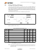
In this mode the upper address inputs are not decoded, and any write to the LAN9221/LAN9221i will
write the TX Data FIFO. This mode is enabled when FIFO_SEL is driven high during a write access.
This is normally accomplished by connecting the FIFO_SEL signal to a high-order address line. This
mode is useful when the host processor must increment its address when accessing the
LAN9221/LAN9221i. Timing is identical to a PIO write, and the FIFO_SEL signal has the same timing
characteristics as the address lines.
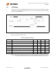
Note: The “Data Bus” width is 16 bits.
Note: A TX Data FIFO Direct PIO Write cycle begins when both nCS and nWR are asserted. The
cycle ends when either or both nCS and nWR are deasserted. They may be asserted and
deasserted in any order.
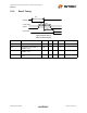
Figure 6.7 TX Data FIFO Direct PIO Write Timing
Table 6.8 TX Data FIFO Direct PIO Write Timing
SYMBOL DESCRIPTION MIN TYP MAX UNITS
t
cycle
Write Cycle Time 45 ns
t
csl
nCS, nWR Assertion Time 32 ns
t
csh
nCS, nWR Deassertion Time 13 ns
t
asu
Address, FIFO_SEL Setup to nCS, nWR Assertion 0 ns
t
ah
Address, FIFO_SEL Hold Time 0 ns
t
dsu
Data Setup to nCS, nWR Deassertion 7 ns
t
dh
Data Hold Time 0 ns
Data Bus
nCS, nWR
FIFO
_
SEL
A
[
2:1
]