
Datasheet


High-Performance 16-bit Non-PCI 10/100 Ethernet Controller with Variable Voltage I/O
Datasheet
Revision 2.9 (03-01-12) 128 SMSC LAN9221/LAN9221i
DATASHEET
6.2.1 Special Restrictions on Back-to-Back Write/Read Cycles
It is important to note that there are specific restrictions on the timing of back-to-back write-read
operations. These restrictions concern reading the control registers after any write cycle to the
LAN9221/LAN9221i device. In many cases there is a required minimum delay between writing to the
LAN9221/LAN9221i, and the subsequent side effect (change in the control register value). For
example, when writing to the TX Data FIFO, it takes up to 135ns for the level indication to change in
the TX_FIFO_INF register.
In order to prevent the host from reading stale data after a write operation, minimum wait periods must
be enforced. These periods are specified in Table 6.1, "Read After Write Timing Rules". The host
processor is required to wait the specified period of time after any write to the LAN9221/LAN9221i
before reading the resource specified in the table. These wait periods are for read operations that
immediately follow any write cycle. Note that the required wait period is dependant upon the register
being read after the write.
Performing "dummy" reads of the BYTE_TEST register is a convenient way to guarantee that the
minimum write-to-read timing restriction is met. Table 6.1 also shows the number of dummy reads that
are required before reading the register indicated. The number of BYTE_TEST reads in this table is
based on the minimum timing for Tcycle (45ns). For microprocessors with slower busses the number
of reads may be reduced as long as the total time is equal to, or greater than the time specified in the
table. Note that dummy reads of the BYTE_TEST register are not required as long as the minimum
time period is met.
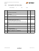
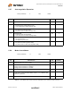
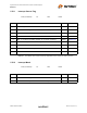
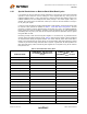
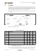
Table 6.1 Read After Write Timing Rules
REGISTER NAME
MINIMUM WAIT TIME FOR READ
FOLLOWING ANY WRITE CYCLE
(IN NS)
NUMBER OF BYTE_TEST
READS
(ASSUMING T
CYCLE
OF 45NS)
ID_REV 0 0
IRQ_CFG 135 3
INT_STS 90 2
INT_EN 45 1
BYTE_TEST 0 0
FIFO_INT 45 1
RX_CFG 45 1
TX_CFG 45 1
HW_CFG 45 1
RX_DP_CTRL 45 1
RX_FIFO_INF 0 0
TX_FIFO_INF 135 3
PMT_CTRL 315 7
GPIO_CFG 45 1
GPT_CFG 45 1
GPT_CNT 135 3
WORD_SWAP 45 1