
Datasheet


High-Performance 16-bit Non-PCI 10/100 Ethernet Controller with Variable Voltage I/O
Datasheet
Revision 2.9 (03-01-12) 16 SMSC LAN9221/LAN9221i
DATASHEET
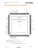
2.1 Pin List
Note: The pin names for the twisted pair pins shown above apply to a normal connection. If HP Auto-
MDIX is enabled and a reverse connection is detected, or a reverse connection is manually
selected, the input pins become outputs, and vice-versa, as indicated in the descriptions.
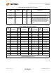
Table 2.1 Host Bus Interface Signals
NAME SYMBOL
BUFFER
TYPE
#
PINS DESCRIPTION
Host Data D[15:0] VIS/VO8 16 Bi-directional data port.
Host Address A[7:1] VIS 7 7-bit Address Port. Used to select Internal CSR’s and
TX and RX FIFOs.
Read Strobe nRD VIS 1 Active low strobe to indicate a read cycle.
Write Strobe nWR VIS 1 Active low strobe to indicate a write cycle. This signal,
qualified with nCS, is also used to wakeup the
LAN9221/LAN9221i when it is in a reduced power
state.
Chip Select nCS VIS 1 Active low signal used to qualify read and write
operations. This signal qualified with nWR is also used
to wakeup the LAN9221/LAN9221i when it is in a
reduced power state.
Interrupt
Request
IRQ VO8/
VOD8
1 Programmable Interrupt request. Programmable
polarity, source and buffer types.
FIFO Select FIFO_SEL VIS 1 When driven high all accesses to the
LAN9221/LAN9221i are to the RX or TX Data FIFOs.
In this mode, the A[7:3] upper address inputs are
ignored.
Table 2.2 LAN Interface Signals
NAME SYMBOL
BUFFER
TYPE
NUM
PINS DESCRIPTION
TPO+ TPO+ AO 1 Transmit Positive Output (normal)
Receive Positive Input (reversed)
TPO- TPO- AO 1 Transmit Negative Output (normal)
Receive Negative Input (reversed)
TPI+ TPI+ AI 1 Receive Positive Input (normal)
Transmit Positive Input (reversed)
TPI- TPI- AI 1 Receive Negative Input (normal)
Transmit Negative Output (reversed)
PHY External Bias
Resistor
EXRES AI 1 Must be connected to ground through a 12.4K
ohm 1% resistor.