
Datasheet
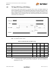

High-Performance 16-bit Non-PCI 10/100 Ethernet Controller with Variable Voltage I/O
Datasheet
Revision 2.9 (03-01-12) 132 SMSC LAN9221/LAN9221i
DATASHEET
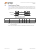
6.5 RX Data FIFO Direct PIO Reads
In this mode the upper address inputs are not decoded, and any read of the LAN9221/LAN9221i will
read the RX Data FIFO. This mode is enabled when FIFO_SEL is driven high during a read access.
This is normally accomplished by connecting the FIFO_SEL signal to high-order address line. This
mode is useful when the host processor must increment its address when accessing the
LAN9221/LAN9221i. Timing is identical to a PIO read, and the FIFO_SEL signal has the same timing
characteristics as the address lines.
Note that address lines A[2:1] are still used, and address bits A[7:3] are ignored.
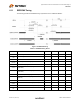
Note: The “Data Bus” width is 16 bits.
Note 6.4 When VDDVARIO is 3.3V or 2.5V, the maximum T
doff
time is 7ns. When VDDVARIO is
1.8V, the maximum T
doff
time is 9ns.
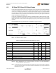
Note: An RX Data FIFO Direct PIO Read cycle begins when both nCS and nRD are asserted. The
cycle ends when either or both nCS and nRD are de-asserted. They may be asserted and de-
asserted in any order.
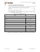
Figure 6.4 RX Data FIFO Direct PIO Read Cycle Timing
Table 6.5 RX Data FIFO Direct PIO Read Timing
SYMBOL DESCRIPTION MIN TYP MAX UNITS
t
cycle
Read Cycle Time 45 ns
t
csl
nCS, nRD Assertion Time 32 ns
t
csh
nCS, nRD Deassertion Time 13 ns
t
csdv
nCS, nRD Valid to Data Valid 30 ns
t
asu
Address, FIFO_SEL Setup to nCS, nRD Valid 0 ns
t
ah
Address, FIFO_SEL Hold Time 0 ns
t
don
Data Buffer Turn On Time 0 ns
t
doff
Data Buffer Turn Off Time Note 6.4 ns
t
doh
Data Output Hold Time 0 ns
Data Bus
nCS, nRD
FIFO
_
SEL
A
[
2:1]