
Datasheet


dsPIC33FJ32MC302/304, dsPIC33FJ64MCX02/X04 AND dsPIC33FJ128MCX02/X04
DS70291G-page 224 © 2007-2012 Microchip Technology Inc.
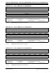
REGISTER 16-9: PxFLTACON: FAULT A CONTROL REGISTER
(1)
U-0 U-0 R/W-0 R/W-0 R/W-0 R/W-0 R/W-0 R/W-0
— — FAOV3H FAOV3L FAOV2H FAOV2L FAOV1H FAOV1L
bit 15 bit 8
R/W-0 U-0 U-0 U-0 U-0 R/W-0 R/W-0 R/W-0
FLTAM
— — — — FAEN3 FAEN2 FAEN1
bit 7 bit 0
Legend:
R = Readable bit W = Writable bit U = Unimplemented bit, read as ‘0’
-n = Value at POR ‘1’ = Bit is set ‘0’ = Bit is cleared x = Bit is unknown
bit 15-14 Unimplemented: Read as ‘0’
bit 13-8 FAOVxH<3:1>:FAOVxL<3:1>: Fault Input A PWM Override Value bits
1 = The PWM output pin is driven active on an external Fault input event
0 = The PWM output pin is driven inactive on an external Fault input event
bit 7 FLTAM: Fault A Mode bit
1 = The Fault A input pin functions in the Cycle-by-Cycle mode
0 = The Fault A input pin latches all control pins to the programmed states in PxFLTACON<13:8>
bit 6-3 Unimplemented: Read as ‘0’
bit 2 FAEN3: Fault Input A Enable bit
1 = PWMxH3/PWMxL3 pin pair is controlled by Fault Input A
0 = PWMxH3/PWMxL3 pin pair is not controlled by Fault Input A
bit 1 FAEN2: Fault Input A Enable bit
1 = PWMxH2/PWMxL2 pin pair is controlled by Fault Input A
0 = PWMxH2/PWMxL2 pin pair is not controlled by Fault Input A
bit 0 FAEN1: Fault Input A Enable bit
1 = PWMxH1/PWMxL1 pin pair is controlled by Fault Input A
0 = PWMxH1/PWMxL1 pin pair is not controlled by Fault Input A
Note 1: PWM2 supports only one PWM I/O pin pair.