
Datasheet


© 2007-2012 Microchip Technology Inc. DS70292G-page 95
dsPIC33FJ32GP302/304, dsPIC33FJ64GPX02/X04, AND dsPIC33FJ128GPX02/X04
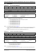
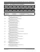
REGISTER 7-4: INTCON2: INTERRUPT CONTROL REGISTER 2
R/W-0 R-0 U-0 U-0 U-0 U-0 U-0 U-0
ALTIVT DISI
— — — — — —
bit 15 bit 8
U-0 U-0 U-0 U-0 U-0 R/W-0 R/W-0 R/W-0
— — — — — INT2EP INT1EP INT0EP
bit 7 bit 0
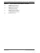
Legend:
R = Readable bit W = Writable bit U = Unimplemented bit, read as ‘0’
-n = Value at POR ‘1’ = Bit is set ‘0’ = Bit is cleared x = Bit is unknown
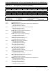
bit 15 ALTIVT: Enable Alternate Interrupt Vector Table bit
1 = Use alternate vector table
0 = Use standard (default) vector table
bit 14 DISI: DISI Instruction Status bit
1 = DISI instruction is active
0 = DISI instruction is not active
bit 13-3 Unimplemented: Read as ‘0’
bit 2 INT2EP: External Interrupt 2 Edge Detect Polarity Select bit
1 = Interrupt on negative edge
0 = Interrupt on positive edge
bit 1 INT1EP: External Interrupt 1 Edge Detect Polarity Select bit
1 = Interrupt on negative edge
0 = Interrupt on positive edge
bit 0 INT0EP: External Interrupt 0 Edge Detect Polarity Select bit
1 = Interrupt on negative edge
0 = Interrupt on positive edge