
Datasheet


dsPIC33FJ32GP302/304, dsPIC33FJ64GPX02/X04, AND dsPIC33FJ128GPX02/X04
DS70292G-page 82 © 2007-2012 Microchip Technology Inc.
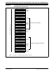
FIGURE 6-2: SYSTEM RESET TIMING
Reset
Run
Device Status
V
DD
VPOR
Vbor
VBOR
POR
BOR
SYSRST
TPWRT
TPOR
TBOR
Oscillator Clock
T
OSCD TOST
TLOCK
Time
FSCM
T
FSCM
1
2
3
4
5
6
Note 1: POR: A POR circuit holds the device in Reset when the power supply is turned on. The POR circuit is active
until V
DD crosses the VPOR threshold and the delay TPOR has elapsed.
2: BOR: The on-chip voltage regulator has a BOR circuit that keeps the device in Reset until V
DD crosses the
V
BOR threshold and the delay TBOR has elapsed. The delay TBOR ensures the voltage regulator output
becomes stable.
3: PWRT Timer: The programmable power-up timer continues to hold the processor in Reset for a specific
period of time (T
PWRT) after a BOR. The delay TPWRT ensures that the system power supplies have stabilized
at the appropriate level for full-speed operation. After the delay T
PWRT has elapsed, the SYSRST becomes
inactive, which in turn enables the selected oscillator to start generating clock cycles.
4: Oscillator Delay: The total delay for the clock to be ready for various clock source selections are given in
Table 6-1. Refer to Section 9.0 “Oscillator Configuration” for more information.
5: When the oscillator clock is ready, the processor begins execution from location 0x000000. The user
application programs a GOTO instruction at the reset address, which redirects program execution to the
appropriate start-up routine.
6: The Fail-Safe Clock Monitor (FSCM), if enabled, begins to monitor the system clock when the system clock
is ready and the delay T
FSCM elapsed.