
Datasheet


dsPIC33FJ32GP302/304, dsPIC33FJ64GPX02/X04, AND dsPIC33FJ128GPX02/X04
DS70292G-page 60 © 2007-2012 Microchip Technology Inc.
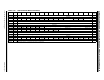
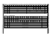
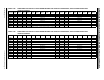
TABLE 4-33: SYSTEM CONTROL REGISTER MAP
File Name Addr Bit 15 Bit 14 Bit 13 Bit 12 Bit 11 Bit 10 Bit 9 Bit 8 Bit 7 Bit 6 Bit 5 Bit 4 Bit 3 Bit 2 Bit 1 Bit 0
All
Resets
RCON 0740 TRAPR IOPUWR — — — — CM VREGS EXTR SWR SWDTEN WDTO SLEEP IDLE BOR POR
xxxx
(1)
OSCCON
0742 — COSC<2:0> — NOSC<2:0> CLKLOCK IOLOCK LOCK —CF— LPOSCEN OSWEN 0300
(2)
CLKDIV
0744 ROI DOZE<2:0> DOZEN FRCDIV<2:0> PLLPOST<1:0> — PLLPRE<4:0> 3040
PLLFBD
0746 — — — — — — — PLLDIV<8:0> 0030
OSCTUN
0748 — — — — — — — — — — TUN<5:0> 0000
ACLKCON
074A
— — SELACLK AOSCMD<1:0> APSTSCLR<2:0> ASRCSEL — — — — — — — 0000
Legend: x = unknown value on Reset, — = unimplemented, read as ‘0’. Reset values are shown in hexadecimal.
Note 1: RCON register Reset values dependent on type of Reset.
2: OSCCON register Reset values dependent on the FOSC Configuration bits and by type of Reset.
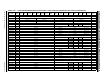
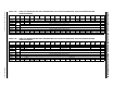
TABLE 4-34: SECURITY REGISTER MAP
(1)
File Name Addr Bit 15 Bit 14 Bit 13 Bit 12 Bit 11 Bit 10 Bit 9 Bit 8 Bit 7 Bit 6 Bit 5 Bit 4 Bit 3 Bit 2 Bit 1 Bit 0
All
Resets
BSRAM 0750 — — — — — — — — — — — — — IW_BSR IR_BSR RL_BSR
0000
SSRAM 0752 — — — — — — — — — — — — — IW_ SSR
IR_SSR
RL_SSR
0000
Legend: x = unknown value on Reset, — = unimplemented, read as ‘0’. Reset values are shown in hexadecimal.
Note 1: This register is not present in devices with 4K RAM and 32K Flash memory.
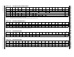
TABLE 4-35: NVM REGISTER MAP
File Name Addr Bit 15 Bit 14 Bit 13 Bit 12 Bit 11 Bit 10 Bit 9 Bit 8 Bit 7 Bit 6 Bit 5 Bit 4 Bit 3 Bit 2 Bit 1 Bit 0
All
Resets
NVMCON 0760 WR WREN WRERR — — — — — —ERASE— —NVMOP<3:0>
0000
NVMKEY 0766
— — — — — — — — NVMKEY<7:0>
0000
Legend: x = unknown value on Reset, — = unimplemented, read as ‘0’. Reset values are shown in hexadecimal.
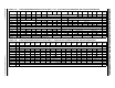
TABLE 4-36: PMD REGISTER MAP
File Name Addr Bit 15 Bit 14 Bit 13 Bit 12 Bit 11 Bit 10 Bit 9 Bit 8 Bit 7 Bit 6 Bit 5 Bit 4 Bit 3 Bit 2 Bit 1 Bit 0
All
Resets
PMD1 0770 T5MD T4MD T3MD T2MD T1MD
— — DCIMD
I2C1MD U2MD U1MD SPI2MD SPI1MD
—
C1MD AD1MD 0000
PMD2 0772 IC8MD IC7MD
— — — —IC2MDIC1MD— — — — OC4MD OC3MD OC2MD OC1MD 0000
PMD3 0774
— — — — — CMPMD RTCCMD PMPMD CRCMD DAC1MD — — — — — — 0000
Legend: x = unknown value on Reset, — = unimplemented, read as ‘0’. Reset values are shown in hexadecimal.