
Datasheet


dsPIC33FJ32GP302/304, dsPIC33FJ64GPX02/X04, AND dsPIC33FJ128GPX02/X04
DS70292G-page 386 © 2007-2012 Microchip Technology Inc.
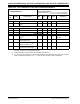
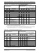
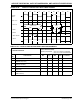
TABLE 30-46: AUDIO DAC MODULE SPECIFICATIONS
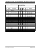
TABLE 30-45: ADC CONVERSION (10-BIT MODE) TIMING REQUIREMENTS
AC CHARACTERISTICS
Standard Operating Conditions: 3.0V to 3.6V
(unless otherwise stated)
Operating temperature -40°C ≤ TA ≤ +85°C for Industrial
-40°C ≤T
A ≤+125°C for Extended
Param
No.
Symbol Characteristic Min. Typ
(2)
Max. Units Conditions
Clock Parameters
(1)
AD50 TAD ADC Clock Period 76 — — ns —
AD51 t
RC ADC Internal RC Oscillator Period — 250 — ns —
Conversion Rate
AD55 t
CONV Conversion Time — 12 TAD —— —
AD56 F
CNV Throughput Rate — — 1.1 Msps —
AD57 T
SAMP Sample Time 2 TAD ——— —
Timing Parameters
AD60 t
PCS Conversion Start from Sample
Trigger
(2)
2 TAD —3 TAD — Auto-Convert Trigger
not selected
AD61 tPSS Sample Start from Setting
Sample (SAMP) bit
(2)
2 TAD —3 TAD ——
AD62 t
CSS Conversion Completion to
Sample Start (ASAM = 1)
(2)
— 0.5 TAD —— —
AD63 tDPU Time to Stabilize Analog Stage
from ADC Off to ADC On
(2,3)
——20μs—
Note 1: Because the sample caps eventually loses charge, clock rates below 10 kHz may affect linearity
performance, especially at elevated temperatures.
2: These parameters are characterized but not tested in manufacturing.
3: The t
DPU is the time required for the ADC module to stabilize at the appropriate level when the module is
turned on ADON bit (AD1CON1<15>) = 1. During this time, the ADC result is indeterminate.
AC/DC CHARACTERISTICS
Standard Operating Conditions: 3.0V to 3.6V
(unless otherwise stated)
Operating temperature -40°C ≤ T
A ≤ +85°C for Industrial
-40°C ≤TA ≤+125°C for Extended
Param
No.
Symbol Characteristic Min. Typ Max. Units Conditions
Clock Parameters
DA01 V
OD+ Positive Output Differential
Voltage
11.152 VVOD+ = VDACH – VDACL
See Note 1, 2
DA02 VOD- Negative Output Differential
Voltage
-2 -1.15 -1 V VOD- = VDACL – VDACH
See Note 1, 2
DA03 V
RES Resolution — 16 — bits —
DA04 GERR Gain Error — 3.1 — % —
DA08 F
DAC Clock frequency — — 25.6 MHz —
DA09 F
SAMP Sample Rate 0 — 100 kHz —
DA10 F
INPUT Input data frequency 0 — 45 kHz Sampling frequency = 100 kHz
DA11 T
INIT Initialization period 1024 — — Clks Time before first sample
DA12 SNR Signal-to-Noise Ratio — 61 dB Sampling frequency = 96 kHz
Note 1: Measured V
DACH and VDACL output with respect to VSS, with 15 µA load and FORM bit (DACXCON<8>) = 0.
2: This parameter is tested at -40°C ≤ T
A ≤ 85°C only.