
Datasheet


dsPIC33FJ32GP302/304, dsPIC33FJ64GPX02/X04, AND dsPIC33FJ128GPX02/X04
DS70292G-page 350 © 2007-2012 Microchip Technology Inc.
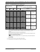
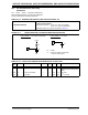
FIGURE 30-2: EXTERNAL CLOCK TIMING
Q1 Q2 Q3 Q4
OSC1
CLKO
Q1 Q2 Q3 Q4
OS20
OS25
OS30 OS30
OS40
OS41
OS31 OS31
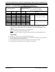
TABLE 30-16: EXTERNAL CLOCK TIMING REQUIREMENTS
AC CHARACTERISTICS
Standard Operating Conditions: 3.0V to 3.6V
(unless otherwise stated)
Operating temperature -40°C ≤ TA ≤ +85°C for Industrial
-40°C ≤TA ≤+125°C for Extended
Param
No.
Symbol Characteristic Min Typ
(1)
Max Units Conditions
OS10 FIN External CLKI Frequency
(External clocks allowed only
in EC and ECPLL modes)
DC — 40 MHz EC
Oscillator Crystal Frequency 3.5
10
—
3.5
—
—
—
—
10
40
33
10
MHz
MHz
kHz
MHz
XT
HS
SOSC
AUX_OSC_F
IN
OS20 TOSC TOSC = 1/FOSC 12.5 — DC ns —
OS25 T
CY Instruction Cycle Time
(2)
25 — DC ns —
OS30 TosL,
Tos H
External Clock in (OSC1)
High or Low Time
0.375 x TOSC — 0.625 x TOSC ns EC
OS31 TosR,
Tos F
External Clock in (OSC1)
Rise or Fall Time
——20nsEC
OS40 TckR CLKO Rise Time
(3)
—5.2—ns —
OS41 TckF CLKO Fall Time
(3)
—5.2—ns —
OS42 GM External Oscillator
Transconductance
(4)
14 16 18 mA/V VDD = 3.3V
T
A = +25ºC
Note 1: Data in “Typ” column is at 3.3V, 25°C unless otherwise stated.
2: Instruction cycle period (TCY) equals two times the input oscillator time-base period. All specified values
are based on characterization data for that particular oscillator type under standard operating conditions
with the device executing code. Exceeding these specified limits may result in an unstable oscillator
operation and/or higher than expected current consumption. All devices are tested to operate at “min.”
values with an external clock applied to the OSC1/CLKI pin. When an external clock input is used, the
“max.” cycle time limit is “DC” (no clock) for all devices.
3: Measurements are taken in EC mode. The CLKO signal is measured on the OSC2 pin.
4: Data for this parameter is Preliminary. This parameter is characterized, but not tested in manufacturing.