
Datasheet


© 2007-2012 Microchip Technology Inc. DS70292G-page 347
dsPIC33FJ32GP302/304, dsPIC33FJ64GPX02/X04, AND dsPIC33FJ128GPX02/X04
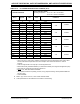
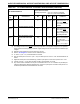
TABLE 30-10: DC CHARACTERISTICS: I/O PIN OUTPUT SPECIFICATIONS
DC CHARACTERISTICS
Standard Operating Conditions: 3.0V to 3.6V
(unless otherwise stated)
Operating temperature -40°C ≤ TA ≤ +85°C for Industrial
-40°C ≤ T
A ≤ +125°C for Extended
Param. Symbol Characteristic Min. Typ. Max. Units Conditions
DO10 V
OL
Output Low Voltage
I/O Pins:
2x Sink Driver Pins - RA2, RA7-
RA10, RB10, RB11, RB7, RB4,
RC3-RC9
——0.4V
I
OL ≤ 3 mA, VDD = 3.3V
See Note 1
Output Low Voltage
I/O Pins:
4x Sink Driver Pins - RA0, RA1,
RB0-RB3, RB5, RB6, RB8, RB9,
RB12-RB15, RC0-RC2
——0.4V
I
OL ≤ 6 mA, VDD = 3.3V
See Note 1
Output Low Voltage
I/O Pins:
8x Sink Driver Pins - RA3, RA4
——0.4V
I
OL ≤ 10 mA, VDD = 3.3V
See Note 1
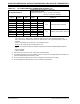
DO20 V
OH
Output High Voltage
I/O Pins:
2x Source Driver Pins - RA2,
RA7-RA10, RB4, RB7, RB10,
RB11, RC3-RC9
2.4 — — V
I
OH ≥ -3 mA, VDD = 3.3V
See Note 1
Output High Voltage
I/O Pins:
4x Source Driver Pins - RA0,
RA1, RB0-RB3, RB5, RB6, RB8,
RB9, RB12-RB15, RC0-RC2
2.4 — — V
I
OH ≥ -6 mA, VDD = 3.3V
See Note 1
Output High Voltage
I/O Pins:
8x Source Driver Pins - RA4,
RA3
2.4 — — V
I
OH ≥ -10 mA, VDD = 3.3V
See Note 1
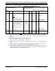
DO20A V
OH1
Output High Voltage
I/O Pins:
2x Source Driver Pins - RA2,
RA7-RA10, RB4, RB7, RB10,
RB11, RC3-RC9
1.5 — —
V
I
OH ≥ -6 mA, VDD = 3.3V
See Note 1
2.0 — —
I
OH ≥ -5 mA, VDD = 3.3V
See Note 1
3.0 — —
I
OH ≥ -2 mA, VDD = 3.3V
See Note 1
Output High Voltage
4x Source Driver Pins - RA0,
RA1, RB0-RB3, RB5, RB6, RB8,
RB9, RB12-RB15, RC0-RC2
1.5 — —
V
I
OH ≥ -12 mA, VDD = 3.3V
See Note 1
2.0 — —
I
OH ≥ -11 mA, VDD = 3.3V
See Note 1
3.0 — —
I
OH ≥ -3 mA, VDD = 3.3V
See Note 1
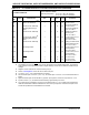
Output High Voltage
I/O Pins:
8x Source Driver Pins - RA3,
RA4
1.5 — —
V
I
OH ≥ -16 mA, VDD = 3.3V
See Note 1
2.0 — —
I
OH ≥ -12 mA, VDD = 3.3V
See Note 1
3.0 — —
I
OH ≥ -4 mA, VDD = 3.3V
See Note 1
Note 1: Parameters are characterized, but not tested.