
Datasheet


© 2007-2012 Microchip Technology Inc. DS70292G-page 345
dsPIC33FJ32GP302/304, dsPIC33FJ64GPX02/X04, AND dsPIC33FJ128GPX02/X04
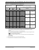
IIL Input Leakage Current
(2,3)
DI50 I/O pins 5V Tolerant
(4)
——±2μAVSS ≤ VPIN ≤ VDD,
Pin at high-impedance
DI51 I/O Pins Not 5V Tolerant
(4)
(Excluding AN9 through
AN12)
——±1μAVSS ≤ VPIN ≤ VDD,
Pin at high-impedance,
40°C ≤ T
A ≤+85°C
DI51a I/O Pins Not 5V Tolerant
(4)
——±2μA Shared with external
reference pins,
40°C ≤ T
A ≤ +85°C
DI51b I/O Pins Not 5V Tolerant
(4)
(Excluding AN9 through
AN12)
——±3.5μAV
SS ≤ VPIN ≤ VDD, Pin at
high-impedance,
-40°C ≤T
A ≤+125°C
DI51c I/O Pins Not 5V Tolerant
(4)
——±8μA Analog pins shared with
external reference pins,
-40°C ≤T
A ≤+125°C
DI51d AN9 through AN12 — — ±11 μAV
SS ≤ VPIN ≤ VDD, Pin at
high-impedance,
-40°C ≤T
A ≤+85°C
DI51e AN9 through AN12 — — ±13 μAV
SS ≤ VPIN ≤ VDD, Pin at
high-impedance,
-40°C ≤TA ≤+125°C
DI55 MCLR —
—
±2 μAVSS ≤ VPIN ≤ VDD
DI56 OSC1 — — ±2 μAVSS ≤ VPIN ≤ VDD,
XT and HS modes
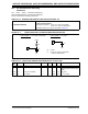
TABLE 30-9: DC CHARACTERISTICS: I/O PIN INPUT SPECIFICATIONS (CONTINUED)
DC CHARACTERISTICS
Standard Operating Conditions: 3.0V to 3.6V
(unless otherwise stated)
Operating temperature -40°C ≤ TA ≤ +85°C for Industrial
-40°C ≤TA ≤+125°C for Extended
Param
No.
Symbol Characteristic Min Typ
(1)
Max Units Conditions
Note 1: Data in “Typ” column is at 3.3V, 25°C unless otherwise stated.
2: The leakage current on the MCLR
pin is strongly dependent on the applied voltage level. The specified
levels represent normal operating conditions. Higher leakage current can be measured at different input
voltages.
3: Negative current is defined as current sourced by the pin.
4: See the “Pin Diagrams” section for the 5V tolerant I/O pins.
5: V
IL source < (VSS – 0.3). Characterized but not tested.
6: Non-5V tolerant pins V
IH source > (VDD + 0.3), 5V tolerant pins VIH source > 5.5V. Characterized but not
tested.
7: Digital 5V tolerant pins cannot tolerate any “positive” input injection current from input sources > 5.5V.
8: Injection currents > | 0 | can affect the ADC results by approximately 4-6 counts.
9: Any number and/or combination of I/O pins not excluded under I
ICL or IICH conditions are permitted pro-
vided the mathematical “absolute instantaneous” sum of the input injection currents from all pins do not
exceed the specified limit. Characterized but not tested.