
Datasheet


dsPIC33FJ32GP302/304, dsPIC33FJ64GPX02/X04, AND dsPIC33FJ128GPX02/X04
DS70292G-page 314 © 2007-2012 Microchip Technology Inc.
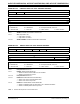
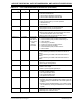
REGISTER 26-6: PADCFG1: PAD CONFIGURATION CONTROL REGISTER
U-0 U-0 U-0 U-0 U-0 U-0 U-0 U-0
— — — — — — — —
bit 15 bit 8
U-0 U-0 U-0 U-0 U-0 U-0 R/W-0 R/W-0
— — — — — — RTSECSEL
(1)
PMPTTL
bit 7 bit 0
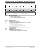
Legend:
R = Readable bit W = Writable bit U = Unimplemented bit, read as ‘0’
-n = Value at POR ‘1’ = Bit is set ‘0’ = Bit is cleared x = Bit is unknown
bit 15-2 Unimplemented: Read as ‘0’
bit 1 RTSECSEL: RTCC Seconds Clock Output Select bit
(1)
1 = RTCC seconds clock is selected for the RTCC pin
0 = RTCC alarm pulse is selected for the RTCC pin
bit 0 PMPTTL: PMP Module TTL Input Buffer Select bit
1 = PMP module uses TTL input buffers
0 = PMP module uses Schmitt Trigger input buffers
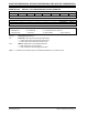
Note 1: To enable the actual RTCC output, the RTCOE bit (RCFGCAL<10>) needs to be set.